|
|

This appendix provides the following pinout information:
The console port is configured as data communications equipment (DCE), and the auxiliary port is configured as data terminal equipment (DTE). The console and auxiliary ports both use RJ-45 connectors. RJ-45-to-DB-25 adapters are available for connection to modems and other external communications equipment. Both ports are configured as asynchronous serial ports.
Following are the pinouts for the console port (see Table C-1), the auxiliary port (see Table C-2), and the adapter (see Table C-16 and Table C-17).
Table C-1 Console Port Pinouts (RJ-45)
| Console Port (DTE) | ||
|---|---|---|
| Pin(1) | Signal | Input/Output |
| 1 | -- | -- |
| 2 | DTR | Output |
| 3 | TxD | Output |
| 4 | GND | -- |
| 5 | GND | -- |
| 6 | RxD | Input |
| 7 | DSR | Input |
| 8 | -- | -- |
Table C-2 Auxiliary Port Pinouts (RJ-45)
| Auxiliary Port (DTE) | ||
|---|---|---|
| Pin(1) | Signal | Input/Output |
| 1 | RTS | Output |
| 2 | DTR | Output |
| 3 | TXD | Output |
| 4 | GND | -- |
| 5 | GND | -- |
| 6 | RXD | Input |
| 7 | DSR | Input |
| 8 | CTS | Input |
The following illustrations and tables provide assembly drawings and pinouts for the EIA-530 DCE, and EIA/TIA-232, EIA/TIA-449, V.35, and X.21 DTE and DCE cables.
Figure C-1 shows the EIA-530 serial cable assembly, and Table C-3 lists the pinouts. Arrows indicate signal direction: ---> indicates DTE to DCE, and <--- indicates DCE to DTE.
Figure C-1 EIA-530 Serial Cable Assembly
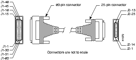
Table C-3 EIA-530 DTE Cable Pinout (DB-60 to DB-25)
| 60 Pin(1) | Signal | 25 Pin | Signal | DirectionDTE DCE(2) |
|---|---|---|---|---|
| J1-11J1-12 | TxD/RxD+TxD/RxD-- | J2-2J2-14 | BA(A), TxD+BA(B), TxD-- | --->---> |
| J1-28J1-27 | RxD/TxD+RxD/TxD-- | J2-3J2-16 | BB(A), RxD+BB(B), RxD-- | <---<--- |
| J1-9J1-10 | RTS/CTS+RTS/CTS-- | J2-4J2-19 | CA(A), RTS+CA(B), RTS-- | --->---> |
| J1-1J1-2 | CTS/RTS+CTS/RTS-- | J2-5J2-13 | CB(A), CTS+ CB(B), CTS-- | <---<--- |
| J1-3J1-4 | DSR/DTR+DSR/DTR-- | J2-6J2-22 | CC(A), DSR+ CC(B), DSR-- | <---<--- |
| J1-46J1-47 | Shield_GNDMODE_2 | J2-1-- | Shield-- | Shorted |
| J1-48J1-49 | GNDMODE_1 | ---- | ---- | Shorted |
| J1-5J1-6 | DCD/DCD+DCD/DCD-- | J2-8J2-10 | CF(A), DCD+CF(B), DCD-- | <---<--- |
| J1-24J1-23 | TxC/RxC+TxC/RxC-- | J2-15J2-12 | DB(A), TxC+DB(B), TxC-- | <---<--- |
| J1-26J1-25 | RxC/TxCE+RxC/TxCE-- | J2-17J2-9 | DD(A), RxC+DD(B), RxC-- | <---<--- |
| J1-44J1-45 | LL/DCDCircuit_GND | J2-18J2-7 | LL Circuit_ GND | --->-- |
| J1-7J1-8 | DTR/DSR+DTR/DSR-- | J2-20J2-23 | CD(A), DTR+CD(B), DTR-- | --->---> |
| J1-13J1-14 | TxCE/TxC+TxCE/TxC-- | J2-24J2-11 | DA(A), TxCE+DA(B), TxCE-- | --->---> |
Figure C-2 shows the EIA/TIA-232 cable assembly; Table C-4 lists the DTE pinout; and Table C-5 lists the DCE pinout. Arrows indicate signal direction: ---> indicates DTE to DCE, and <--- indicates DCE to DTE.
Figure C-2 EIA/TIA-232 Cable Assembly
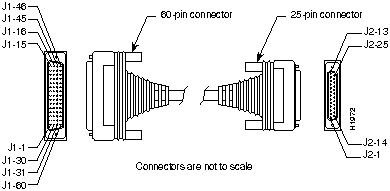
Table C-4 EIA/TIA-232 DTE Cable Pinout (DB-60 to DB-25)
| 60 Pin(1) | Signal | Description | Direction | 25 Pin | Signal |
|---|---|---|---|---|---|
| J1-50J1-51J1-52 | MODE_0GNDMODE_DCE | Shorting group | -- | -- | -- |
| J1-46 | Shield GND | Single | -- | J2-1 | Shield GND |
| J1-41Shield | TxD/RxD-- | Twisted pair no. 5 | --->-- | J2-2Shield | TxD-- |
| J1-36Shield | RxD/TxD-- | Twisted pair no. 9 | <----- | J2-3Shield | RxD-- |
| J1-42Shield | RTS/CTS-- | Twisted pair no. 4 | --->-- | J2-4Shield | RTS-- |
| J1-35Shield | CTS/RTS-- | Twisted pair no. 10 | <----- | J2-5Shield | CTS-- |
| J1-34Shield | DSR/DTR-- | Twisted pair no. 11 | <----- | J2-6Shield | DSR-- |
| J1-45Shield | Circuit GND-- | Twisted pair no. 1 | ---- | J2-7Shield | Circuit GND-- |
| J1-33Shield | DCD/LL-- | Twisted pair no. 12 | <----- | J2-8Shield | DCD-- |
| J1-37Shield | TxC/NIL-- | Twisted pair no. 8 | <----- | J2-15Shield | TxC-- |
| J1-38Shield | RxC/TxCE-- | Twisted pair no. 7 | <----- | J2-17Shield | RxC-- |
| J1-44Shield | LL/DCD-- | Twisted pair no. 2 | --->-- | J2-18Shield | LTST-- |
| J1-43Shield | DTR/DSR-- | Twisted pair no. 3 | --->-- | J2-20Shield | DTR-- |
| J1-39Shield | TxCE/TxC-- | Twisted pair no. 6 | --->-- | J2-24Shield | TxCE-- |
Table C-5 EIA/TIA-232 DCE Cable Pinout (DB-60 to DB-25)
| 60 Pin(1) | Signal | Description | Direction | 25 Pin | Signal |
|---|---|---|---|---|---|
| J1-50J1-51 | MODE_0GND | Shorting group | -- |
-- |
-- |
| J1-46 | Shield GND | Single | -- | J2-1 | Shield GND |
| J1-36Shield | RxD/TxD-- | Twisted pair no. 9 | <----- | J2-2Shield | TxD-- |
| J1-41Shield | TxD/RxD-- | Twisted pair no. 5 | --->-- | J2-3Shield | RxD-- |
| J1-35Shield | CTS/RTS-- | Twisted pair no. 10 | <----- | J2-4Shield | RTS-- |
| J1-42Shield | RTS/CTS-- | Twisted pair no. 4 | --->-- | J2-5Shield | CTS-- |
| J1-43Shield | DTR/DSR-- | Twisted pair no. 3 | --->-- | J2-6Shield | DSR-- |
| J1-45Shield | Circuit GND-- | Twisted pair no. 1 | ---- | J2-7Shield | Circuit GND |
| J1-44Shield | LL/DCD-- | Twisted pair no. 2 | --->-- | J2-8Shield | DCD-- |
| J1-39Shield | TxCE/TxC-- | Twisted pair no. 7 | --->-- | J2-15Shield | TxC-- |
| J1-40Shield | NIL/RxC-- | Twisted pair no. 6 | --->-- | J2-17Shield | RxC-- |
| J1-33Shield | DCD/LL-- | Twisted pair no. 12 | <----- | J2-18Shield | LTST-- |
| J1-34Shield | DSR/DTR-- | Twisted pair no. 11 | <----- | J2-20Shield | DTR-- |
| J1-38Shield | RxC/TxCE-- | Twisted pair no. 8 | <----- | J2-24Shield | TxCE-- |
Figure C-3 shows the EIA/TIA-449 cable assembly; Table C-6 lists the DTE pinout; Table C-7 lists the DCE pinout. Arrows indicate signal direction: ---> indicates DTE to DCE, and <--- indicates DCE to DTE.
Figure C-3 EIA/TIA-449 Cable Assembly
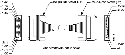
Table C-6 EIA/TIA-449 DTE Cable Pinout (DB-60 to DB-37)
| 60 Pin(1) | Signal | Description | Direction | 37 Pin | Signal |
|---|---|---|---|---|---|
| J1-49J1-48 | MODE_1GND | Shorting group | -- | -- | -- |
| J1-51J1-52 | GNDMODE_DCE | Shorting group | -- | -- | -- |
| J1-46 | Shield_GND | Single | _ | J2-1 | Shield GND |
| J1-11J1-12 | TxD/RxD+TxD/RxD-- | Twisted pair no. 6 | --->---> | J2-4J2-22 | SD+SD-- |
| J1-24J1-23 | TxC/RxC+TxC/RxC-- | Twisted pair no. 9 | <---<--- | J2-5J2-23 | ST+ST-- |
| J1-28J1-27 | RxD/TxD+RxD/TxD-- | Twisted pair no. 11 | <---<--- | J2-6J2-24 | RD+RD-- |
| J1-9J1-10 | RTS/CTS+RTS/CTS-- | Twisted pair no. 5 | --->---> | J2-7J2-25 | RS+RS-- |
| J1-26J1-25 | RxC/TxCE+RxC/TxCE-- | Twisted pair no. 10 | <---<--- | J2-8J2-26 | RT+RT-- |
| J1-1J1-2 | CTS/RTS+CTS/RTS-- | Twisted pair no. 1 | <---<--- | J2-9J2-27 | CS+CS-- |
| J1-44J1-45 | LL/DCDCircuit_GND | Twisted pair no. 12 | --->_ | J2-10J2-37 | LLSC |
| J1-3J1-4 | DSR/DTR+DSR/DTR-- | Twisted pair no. 2 | <---<--- | J2-11J2-29 | DM+DM-- |
| J1-7J1-8 | DTR/DSR+DTR/DSR-- | Twisted pair no. 4 | --->---> | J2-12J2-30 | TR+TR-- |
| J1-5J1-6 | DCD/DCD+DCD/DCD-- | Twisted pair no. 3 | <---<--- | J2-13J2-31 | RR+RR-- |
| J1-13J1-14 | TxCE/TxC+TxCE/TxC-- | Twisted pair no. 7 | --->---> | J2-17J2-35 | TT+TT-- |
| J1-15J1-16 | Circuit_GNDCircuit_GND | Twisted pair no. 9 | ---- | J2-19J2-20 | SGRC |
Table C-7 EIA/TIA-449 DCE Cable Pinout (DB-60 to DB-37)
| 60 Pin(1) | Signal | Description | Direction | 37 Pin | Signal |
|---|---|---|---|---|---|
| J1-49J1-48 | MODE_1GND | Shorting group | -- | -- | -- |
| J1-46 | Shield_GND | Single | -- | J2-1 | Shield GND |
| J1-28J1-27 | RxD/TxD+RxD/TxD-- | Twisted pair no. 11 | <---<--- | J2-4J2-22 | SD+SD-- |
| J1-13J1-14 | TxCE/TxC+TxCE/TxC-- | Twisted pair no. 7 | --->---> | J2-5J2-23 | ST+ST-- |
| J1-11J1-12 | TxD/RxD+TxD/RxD-- | Twisted pair no. 6 | --->---> | J2-6J2-24 | RD+RD-- |
| J1-1J1-2 | CTS/RTS+CTS/RTS-- | Twisted pair no. 1 | <---<--- | J2-7J2-25 | RS+RS-- |
| J1-24J1-23 | TxC/RxC+TxC/RxC-- | Twisted pair no. 9 | --->---> | J2-8J2-26 | RT+RT-- |
| J1-9J1-10 | RTS/CTS+RTS/CTS-- | Twisted pair no. 5 | --->---> | J2-9J2-27 | CS+CS-- |
| J1-29J1-30 | NIL/LLCircuit_GND | Twisted pair no. 12 | --->-- | J2-10J2-37 | LLSC |
| J1-7J1-8 | DTR/DSR+DTR/DSR-- | Twisted pair no. 4 | --->---> | J2-11J2-29 | DM+DM-- |
| J1-3J1-4 | DSR/DTR+DSR/DTR-- | Twisted pair no. 2 | <---<--- | J2-12J2-30 | TR+TR-- |
| J1-5J1-6 | DCD/DCD+DCD/DCD-- | Twisted pair no. 3 | --->---> | J2-13J2-31 | RR+RR-- |
| J1-26J1-25 | RxC/TxCE+RxC/TxCE-- | Twisted pair no. 10 | <---<--- | J2-17J2-35 | TT+TT-- |
| J1-15J1-16 | Circuit_GNDCircuit_GND | Twisted pair no. 8 | __ | J2-19J2-20 | SGRC |
Figure C-4 shows the V.35 cable assembly; Table C-8 lists the DTE pinout; Table C-9 lists the DCE pinout. Arrows indicate signal direction: ---> indicates DTE to DCE, and <--- indicates DCE to DTE.
Figure C-4 V.35 Cable Assembly
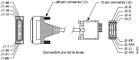
Table C-8 V.35 DTE Cable Pinout (DB-60 to 34-Pin)
| 60 Pin(1) | Signal | Description | Direction | 34 Pin | Signal |
|---|---|---|---|---|---|
| J1-49J1-48 | MODE_1GND | Shorting group | -- | -- | -- |
| J1-50J1-51J1-52 | MODE_0GNDMODE_DCE | Shorting group | -- | -- | -- |
| J1-53J1-54J1-55J1-56 | TxC/NILRxC_TxCERxD/TxDGND | Shorting group | -- | -- | -- |
| J1-46 | Shield_GND | Single | -- | J2-A | Frame GND |
| J1-45Shield | Circuit_GND-- | Twisted pair no. 12 | ---- | J2-BShield | Circuit GND-- |
| J1-42Shield | RTS/CTS-- | Twisted pair no. 9 | --->-- | J2-CShield | RTS-- |
| J1-35Shield | CTS/RTS-- | Twisted pair no. 8 | <----- | J2-DShield | CTS-- |
| J1-34Shield | DSR/DTR-- | Twisted pair no. 7 | <----- | J2-EShield | DSR-- |
| J1-33Shield | DCD/LL-- | Twisted pair no. 6 | <----- | J2-FShield | RLSD-- |
| J1-43Shield | DTR/DSR-- | Twisted pair no. 10 | --->-- | J2-HShield | DTR-- |
| J1-44Shield | LL/DCD-- | Twisted pair no. 11 | --->-- | J2-KShield | LT-- |
| J1-18J1-17 | TxD/RxD+TxD/RxD-- | Twisted pair no. 1 | --->---> | J2-PJ2-S | SD+SD-- |
| J1-28J1-27 | RxD/TxD+RxD/TxD-- | Twisted pair no. 5 | <---<--- | J2-RJ2-T | RD+RD-- |
| J1-20J1-19 | TxCE/TxC+TxCE/TxC-- | Twisted pair no. 2 | --->---> | J2-UJ2-W | SCTE+SCTE-- |
| J1-26J1-25 | RxC/TxCE+RxC/TxCE-- | Twisted pair no. 4 | <---<--- | J2-VJ2-X | SCR+SCR-- |
| J1-24J1-23 | TxC/RxC+TxC/RxC-- | Twisted pair no. 3 | <---<--- | J2-YJ2-AA | SCT+SCT-- |
Table C-9 V.35 DCE Cable Pinout (DB-60 to 34-Pin)
| 60 Pin(1) | Signal | Description | Direction | 34 Pin | Signal |
|---|---|---|---|---|---|
| J1-49J1-48 | MODE_1GND | Shorting group | -- | -- | -- |
| J1-50J1-51 | MODE_0GND | Shorting group | -- | -- | -- |
| J1-53J1-54J1-55J1-56 | TxC/NILRxC_TxCERxD/TxDGND | Shorting group | -- | -- | -- |
| J1-46 | Shield_GND | Single | -- | J2-A | Frame GND |
| J1-45Shield | Circuit_GND-- | Twisted pair no. 12 | ---- | J2-BShield | Circuit GND-- |
| J1-35Shield | CTS/RTS-- | Twisted pair no. 8 | <----- | J2-CShield | RTS-- |
| J1-42Shield | RTS/CTS-- | Twisted pair no. 9 | --->-- | J2-DShield | CTS-- |
| J1-43Shield | DTR/DSR-- | Twisted pair no. 10 | --->-- | J2-EShield | DSR-- |
| J1-44Shield | LL/DCD-- | Twisted pair no. 11 | --->-- | J2-FShield | RLSD-- |
| J1-34Shield | DSR/DTR-- | Twisted pair no. 7 | <----- | J2-HShield | DTR-- |
| J1-33Shield | DCD/LL-- | Twisted pair no. 6 | <----- | J2-KShield | LT-- |
| J1-28J1-27 | RxD/TxD+RxD/TxD-- | Twisted pair no. 5 | <---<--- | J2-PJ2-S | SD+SD-- |
| J1-18J1-17 | TxD/RxD+TxD/RxD-- | Twisted pair no. 1 | --->---> | J2-RJ2-T | RD+RD-- |
| J1-26J1-25 | RxC/TxCE+RxC/TxCE-- | Twisted pair no. 4 | <---<--- | J2-UJ2-W | SCTE+SCTE-- |
| J1-22J1-21 | NIL/RxC+NIL/RxC-- | Twisted pair no. 3 | --->---> | J2-VJ2-X | SCR+SCR-- |
| J1-20J1-19 | TxCE/TxC+TxCE/TxC-- | Twisted pair no. 2 | --->---> | J2-YJ2-AA | SCT+SCT-- |
Figure C-5 shows the X.21 cable assembly; Table C-10 lists the DTE pinout; Table C-11 lists the DCE pinout. Arrows indicate signal direction: ---> indicates DTE to DCE, and <--- indicates DCE to DTE.
Figure C-5 X.21 Cable Assembly
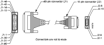
Table C-10 X.21 DTE Cable Pinout (DB-60 to DB-15)
| 60 Pin(1) | Signal | Description | Direction | 15 Pin | Signal |
|---|---|---|---|---|---|
| J1-48J1-47 | GNDMODE_2 | Shorting group | -- | -- | -- |
| J1-51J1-52 | GNDMODE_DCE | Shorting group | -- | -- | -- |
| J1-46 | Shield_GND | Single | -- | J2-1 | Shield GND |
| J1-11J1-12 | TxD/RxD+TxD/RxD-- | Twisted pair no. 3 | --->---> | J2-2J2-9 | Transmit+Transmit-- |
| J1-9J1-10 | RTS/CTS+RTS/CTS-- | Twisted pair no. 2 | --->---> | J2-3J2-10 | Control+Control-- |
| J1-28J1-27 | RxD/TxD+RxD/TxD-- | Twisted pair no. 6 | <---<--- | J2-4J2-11 | Receive+Receive-- |
| J1-1J1-2 | CTS/RTS+CTS/RTS-- | Twisted pair no. 1 | <---<--- | J2-5J2-12 | Indication+Indication-- |
| J1-26J1-25 | RxC/TxCE+RxC/TxCE-- | Twisted pair no. 5 | <---<--- | J2-6J2-13 | Timing+Timing-- |
| J1-15Shield | Control_GND-- | Twisted pair no. 4 | ---- | J2-8Shield | Control GND-- |
Table C-11 X.21 DCE Cable Pinout (DB-60 to DB-15)
| 60 Pin(1) | Signal | Description | Direction | 15 Pin | Signal |
|---|---|---|---|---|---|
| J1-48J1-47 | GNDMODE_2 | Shorting group | -- | -- | -- |
| J1-46 | Shield_GND | Single | -- | J2-1 | Shield GND |
| J1-28J1-27 | RxD/TxD+RxD/TxD-- | Twisted pair no. 6 | <---<--- | J2-2J2-9 | Transmit+Transmit-- |
| J1-1J1-2 | CTS/RTS+CTS/RTS-- | Twisted pair no. 1 | <---<--- | J2-3J2-10 | Control+Control-- |
| J1-11J1-12 | TxD/RxD+TxD/RxD-- | Twisted pair no. 3 | --->---> | J2-4J2-11 | Receive+Receive-- |
| J1-9J1-10 | RTS/CTS+RTS/CTS-- | Twisted pair no. 2 | --->---> | J2-5J2-12 | Indication+Indication-- |
| J1-24J1-23 | TxC/RxC+TxC/RxC-- | Twisted pair no. 4 | --->---> | J2-6J2-13 | Timing+Timing-- |
| J1-15Shield | Control_GND-- | Twisted pair no. 5 | ---- | J2-8Shield | Control GND-- |
Figure C-6 shows an Ethernet (AUI) cable assembly, and Table C-12 lists an AUI cable pinout.
Figure C-6 Ethernet (AUI) Cable Assembly
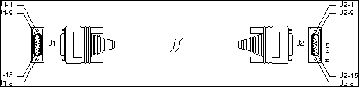
Table C-12 Ethernet (AUI) Cable Pinout (DB-15)
| Pin(1) | Ethernet Circuit | Signal |
|---|---|---|
| 3 | DO-A | Data Out Circuit A |
| 10 | DO-B | Data Out Circuit B |
| 11 | DO-S | Data Out Circuit Shield |
| 5 | DI-A | Data In Circuit A |
| 12 | DI-B | Data In Circuit B |
| 4 | DI-S | Data In Circuit Shield |
| 2 | CI-A | Control In Circuit A |
| 9 | CI-B | Control In Circuit B |
| 1 | CI-S | Control In Circuit Shield |
| 6 | VC | Voltage Common |
| 13 | VP | Voltage Plus |
| 14 | VS | Voltage Shield (L25 and M25) |
| Shell | PG | Protective Ground |
Table C-13 lists the pinout for the Token Ring interface port.
Table C-13 Token Ring Port Pinout (DB-9)
| 9 Pin(1) | Signal |
|---|---|
| 1 | Receive |
| 3 | +5V(2) |
| 5 | Transmit |
| 6 | Receive |
| 9 | Transmit |
Figure C-7 shows the RJ-45 breakout cable with pinouts for the 68-pin SCSI port and the RJ-45 serial port. Table C-14 contains the pinout for the RJ-45 end, and Table C-15 contains the pinout for the 68-pin SCSI type connector.
Figure C-7 Asynchronous Serial Interface Breakout Cable Assembly
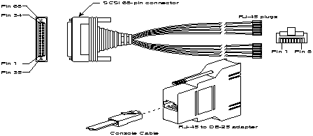
Table C-14 Asynchronous Breakout Cable Pinout (8-Pin RJ-45)
| 8-Pin RJ-45 | Signal | Direction |
|---|---|---|
| 1 | CTS | <--- |
| 2 | DSR/DCD | <--- |
| 3 | RXD | <--- |
| 4 | RXD/GND | --- |
| 5 | TXD/GND | --- |
| 6 | TXD | ---> |
| 7 | DTR | ---> |
| 8 | RTS | ---> |
Table C-15 Asynchronous-Line Cable Pinout (68-Pin SCSI)
| RJ-45 Plug | Pin | Signal | 68-Pin SCSI (J1) |
|---|---|---|---|
| 1 | 1 | CTS | 39 |
| 2 | DSR | 5 | |
| 3 | RXD | 38 | |
| 4 | RXD GND | 4 | |
| 5 | TXD GND | 37 | |
| 6 | TXD | 3 | |
| 7 | DTR | 36 | |
| 8 | RTS | 2 | |
| 2 | 1 | CTS | 43 |
| 2 | DSR | 9 | |
| 3 | RXD | 42 | |
| 4 | RXD GND | 8 | |
| 5 | TXD GND | 41 | |
| 6 | TXD | 7 | |
| 7 | DTR | 40 | |
| 8 | RTS | 6 | |
| 3 | 1 | CTS | 47 |
| 2 | DSR | 13 | |
| 3 | RXD | 46 | |
| 4 | RXD GND | 12 | |
| 5 | TXD GND | 45 | |
| 6 | TXD | 11 | |
| 7 | DTR | 44 | |
| 8 | RTS | 10 | |
| 4 | 1 | CTS | 51 |
| 2 | DSR | 17 | |
| 3 | RXD | 50 | |
| 4 | RXD GND | 16 | |
| 5 | TXD GND | 49 | |
| 6 | TXD | 15 | |
| 7 | DTR | 48 | |
| 8 | RTS | 14 | |
| 5 | 1 | CTS | 55 |
| 2 | DSR | 21 | |
| 3 | RXD | 54 | |
| 4 | RXD GND | 20 | |
| 5 | TXD GND | 53 | |
| 6 | TXD | 19 | |
| 7 | DTR | 52 | |
| 8 | RTS | 18 | |
| 6 | 1 | CTS | 59 |
| 2 | DSR | 25 | |
| 3 | RXD | 58 | |
| 4 | RXD GND | 24 | |
| 5 | TXD GND | 57 | |
| 6 | TXD | 23 | |
| 7 | DTR | 56 | |
| 8 | RTS | 22 | |
| 7 | 1 | CTS | 53 |
| 2 | DSR | 29 | |
| 3 | RXD | 62 | |
| 4 | RXD GND | 28 | |
| 5 | TXD GND | 61 | |
| 6 | TXD | 27 | |
| 7 | DTR | 60 | |
| 8 | RTS | 26 | |
| 8 | 1 | CTS | 67 |
| 2 | DSR | 33 | |
| 3 | RXD | 66 | |
| 4 | RXD GND | 32 | |
| 5 | TXD GND | 65 | |
| 6 | TXD | 31 | |
| 7 | DTR | 64 | |
| 8 | RTS | 30 |
Refer to Table C-16 for a list of the pins used on the RJ-45-to-DB-25 adapters, used with an RJ-45 cable, to connect terminals and modems to the Cisco 2500 series access server. The cable you use may be a roll-over cable or a straight cable.
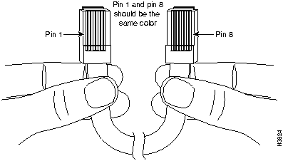
A roll-over cable can be detected by comparing the two modular ends of the cable. Holding the cables in your hand, side-by-side, with the tab at the back, the wire connected to the pin on the outside of the left plug should be the same color as the pin on the outside of the right plug. If your cable was purchased from Cisco, pin 1 will be white on one connector, and pin 8 will be white on the other (a roll-over cable reverses pins 1 and 8, 2 and 7, 3 and 6, and 4 and 5). (See Figure C-8.)
Figure C-8 Identifying a Roll-Over Cable
The Cisco 2500 series access server ships with a rolled cable. Connection to a terminal or a modem will require an RJ-45-to-DB-25 adapter, and possibly a DB-25-to-DB9 adapter. Refer to Table C-17 for the cable and adapter configurations that can be used to connect terminals and modems to the Cisco 2500 series access server.
Table C-16 Pinouts for the RJ-45-to-DB-25 Adapters
| Adapter | DTE M/F Pins(1) | DCE M/F Pins | MMOD Pins(2) |
|---|---|---|---|
| RJ-45 Pins | DB-25 Pins | ||
| 1 | 4 | 5 | 5 |
| 2 | 20 | 6 | 8 |
| 3 | 2 | 3 | 3 |
| 4 | 7 | 7 | 7 |
| 5 | 7 | 7 | 7 |
| 6 | 3 | 2 | 2 |
| 7 | 6 | 20 | 20 |
| 8 | 5 | 4 | 4 |
Table C-17 Asynchronous Device Cabling Options
| Access Server Port | RJ-45 Cable Type | DB-25 Adapter | End Device |
|---|---|---|---|
| Console or auxiliary | Rolled | FDTE(1) | Terminal |
| Console or auxiliary | Straight | FDCE | Terminal |
| Auxiliary or console | Rolled | MMOD(2) | Modem(3) |
|
|
Copyright 1988-1995 © Cisco Systems Inc.