|
|

Cabling Specifications for the Universal Access Server
This appendix provides the following pinout information:
Console and Auxiliary Port Signals and Pinouts
The AS5200 comes with a console and auxiliary cable kit, that contains the cable and adapters you need to connect a console (an ASCII terminal or PC running terminal emulation software) or modem to your AS5200. The console and auxiliary cable kit includes the following items:
For console connections, proceed to the section "Console Port Signals and Pinouts" later in this appendix; for modem connections, proceed to the section "Auxiliary Port Signals and Pinouts" later in this appendix.
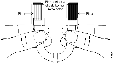
You can identify a roll-over cable by comparing the two modular ends of the cable. Holding the cables side-by-side, with the tab at the back, the wire connected to the pin on the outside of the left plug should be the same color as the wire connected to the pin on the outside of the right plug. (See Figure C-1.) If your cable was purchased from Cisco Systems, pin 1 will be white on one connector, and pin 8 will be white on the other (a roll-over cable reverses pins 1 and 8, 2 and 7, 3 and 6, and 4 and 5).
Figure C-1 : Identifying a Roll-Over Cable
Console Port Signals and Pinouts
Use the RJ-45-to-RJ-45 roll-over cable and RJ-45-to-DB-9 female DTE adapter (labeled Terminal) to connect the console port to a PC running terminal emulation software. Figure C-2 shows how to connect the console port to a PC. Table C-1 lists the pinouts for the asynchronous serial console port, the RJ-45-to-RJ-45 roll-over cable, and the RJ-45-to-DB-9 female DTE adapter (labeled Terminal).
Figure C-2 : Connecting the Console Port to a PC
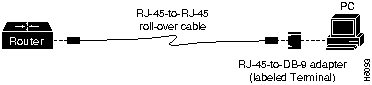
Table C-1 : Console Port Signaling and Cabling Using a DB-9 Adapter
| Console Port (DTE) | RJ-45-to-RJ-45
Roll-Over Cable |
RJ-45-to-DB-9 Terminal Adapter | Console
Device |
|
|---|---|---|---|---|
| Signal | RJ-45 Pin | RJ-45 Pin | DB-9 Pin | Signal |
| RTS | 11 | 8 | 8 | CTS |
| DTR | 2 | 7 | 6 | DSR |
| TxD | 3 | 6 | 2 | RxD |
| GND | 4 | 5 | 5 | GND |
| GND | 5 | 4 | 5 | GND |
| RxD | 6 | 3 | 3 | TxD |
| DSR | 7 | 2 | 4 | DTR |
| CTS | 81 | 1 | 7 | RTS |
Use the RJ-45-to-RJ-45 roll-over cable and RJ-45-to-DB-25 female DTE adapter (labeled Terminal) to connect the console port to a terminal. Figure C-3 shows how to connect the console port to a terminal. Table C-2 lists the pinouts for the asynchronous serial console port, the RJ-45-to-RJ-45 roll-over cable, and the RJ-45-to-DB-25 female DTE adapter (labeled Terminal).
Figure C-3 : Connecting the Console Port to a Terminal
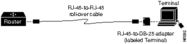
Table C-2 : Console Port Signaling and Cabling Using a DB-25 Adapter
| Console Port (DTE)1 | RJ-45-to-RJ-45 Roll-Over Cable | RJ-45-to-DB-25 Terminal Adapter | Console
Device |
|
|---|---|---|---|---|
| Signal | RJ-45 Pin | RJ-45 Pin | DB-25 Pin | Signal |
| RTS | 12 | 8 | 5 | CTS |
| DTR | 2 | 7 | 6 | DSR |
| TxD | 3 | 6 | 3 | RxD |
| GND | 4 | 5 | 7 | GND |
| GND | 5 | 4 | 7 | GND |
| RxD | 6 | 3 | 2 | TxD |
| DSR | 7 | 2 | 20 | DTR |
| CTS | 81 | 1 | 4 | RTS |
Auxiliary Port Signals and Pinouts
Use the RJ-45-to-RJ-45 roll-over cable and RJ-45-to-DB-25 male DCE adapter (labeled Modem) to connect the auxiliary port to a modem. Figure C-4 shows how to connect the auxiliary port to a modem. Table C-3 lists the pinouts for the asynchronous serial auxiliary port, the RJ-45-to-RJ-45 roll-over cable, and the RJ-45-to-DB-25 male DCE adapter (labeled Modem).
Figure C-4 : Connecting the Auxiliary Port to a Modem
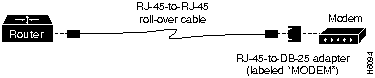
Table C-3 : Auxiliary Port Signaling and Cabling Using a DB-25 Adapter
| AUX Port (DTE) | RJ-45-to-RJ-45
Roll-Over Cable |
RJ-45-to-DB-25 Modem Adapter | Modem | |
|---|---|---|---|---|
| Signal | RJ-45 Pin | RJ-45 Pin | DB-25 Pin | Signal |
| RTS | 1 | 8 | 4 | RTS |
| DTR | 2 | 7 | 20 | DTR |
| TxD | 3 | 6 | 3 | TxD |
| GND | 4 | 5 | 7 | GND |
| GND | 5 | 4 | 7 | GND |
| RxD | 6 | 3 | 2 | RxD |
| DSR | 7 | 2 | 8 | DCD |
| CTS | 8 | 1 | 5 | CTS |
Ethernet Cable Assembly and Pinouts
This section describes the pinouts for the Ethernet ports and cables.
Figure C-5 shows an Ethernet attachment unit interface (AUI) cable assembly, and Table C-4 lists the AUI cable pinouts.
Figure C-5 : Ethernet (AUI) Cable Assembly
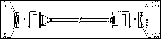
Table C-4 : Ethernet (AUI) Cable Pinouts (DB-15)
| Pin | Ethernet Circuit | Signal |
|---|---|---|
| 3 | DO-A | Data Out Circuit A |
| 10 | DO-B | Data Out Circuit B |
| 11 | DO-S | Data Out Circuit Shield |
| 5 | DI-A | Data In Circuit A |
| 12 | DI-B | Data In Circuit B |
| 4 | DI-S | Data In Circuit Shield |
| 2 | CI-A | Control In Circuit A |
| 9 | CI-B | Control In Circuit B |
| 1 | CI-S | Control In Circuit Shield |
| 6 | VC | Voltage Common |
| 13 | VP | Voltage Plus |
| 14 | VS | Voltage Shield (L25 and M25) |
| Shell | PG | Protective Ground |
Table C-5 lists the T1 PRI card port pinouts. Use a straight-through RJ-48C-to-RJ-48C cable to connect the T1 port to an RJ-48C jack.
Table C-5 : T1 PRI Card Port (RJ-48C) Pinouts
| RJ-48C8 Pin1 | Description |
|---|---|
| 1 | Receive ring from telco |
| 2 | Receive tip from telco |
| 4 | Transmit ring to telco |
| 5 | Transmit tip to telco |
Dual E1 PRI Card Cable Assemblies and Pinouts
Four serial cables are available from Cisco Systems for connecting the E1 PRI card ports. All four have DB-15 connectors on the E1 end and either BNC, DB-15, twinax, or RJ-45 connectors on the network end. Figure C-6, Figure C-7, Figure C-8, and Figure C-9 show the E1 interface cables. Table C-6 lists the pinouts for the E1 interface cables connecting to the Dual E1 PRI card.
Figure C-6 : E1 Interface Cable for 75-Ohm, Unbalanced Connections (with BNC Connectors)
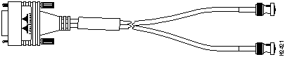
Figure C-7 : E1 Interface Cable for 120-Ohm, Balanced Connections (with DB-15 Connector)
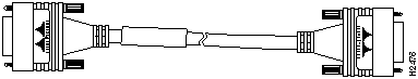
Figure C-8 : E1 Interface Cable for 120-Ohm, Balanced Connections (with Twinax Connectors)
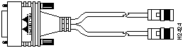
Figure C-9 : E1 Interface Cable for 120-Ohm, Balanced Connections (with RJ-45 Connector)
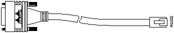
Table C-6 : E1 Interface Cable Pinouts
| CE1 End | Network End | |||||||
|---|---|---|---|---|---|---|---|---|
| DB-151 | BNC | DB-15 | Twinax | RJ-45 | ||||
| Pin | Signal2 | Signal | Pin | Signal | Pin | Signal | Pin | Signal |
| 9 | TX Tip | TX Tip | 1 | TX Tip | TX-1 | TX Tip | 14 | TX Tip |
| 2 | TX Ring | TX Shield | 9 | TX Ring | TX-2 | TX Ring | 52 | TX Ring |
| 10 | TX Shield | -- | 2 | TX Shield | Shield | TX Shield | 36 | TX Shield |
| 8 | RX Tip | RX Tip | 3 | RX Tip | RX-1 | RX Tip | 41 | RX Tip |
| 15 | RX Ring | RX Shield | 11 | RX Ring | RX-2 | RX Ring | 52 | RX Ring |
| 7 | RX Shield | -- | 4 | RX Shield | Shield | RX Shield | 63 | RX Shield |
Synchronous Serial Cable Assemblies and Pinouts
The illustrations and tables in this section provide assembly drawings and pinouts for the EIA-530 data communications equipment (DCE), EIA/TIA-232, EIA/TIA-449, V.35, and X.21 DTE and DCE cables, which are used with the five-in-one synchronous serial WAN port.
Figure C-10 shows the EIA-530 serial cable assembly, and Table C-7 lists the pinouts. Arrows indicate signal direction: a right arrow (--->) indicates DTE to DCE, and a left arrow (<---) indicates DCE to DTE.
Figure C-10 : EIA-530 Serial Cable Assembly
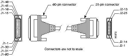
Table C-7 : EIA-530 DTE Cable Pinouts (DB-60 to DB-25)
|
60 Pin |
Signal |
25 Pin |
Signal |
Direction
DTE DCE1 |
|---|---|---|---|---|
| J1-11
J1-12 |
TxD/RxD+
TxD/RxD-- |
J2-2
J2-14 |
BA(A), TxD+
BA(B), TxD-- |
--->
---> |
| J1-28
J1-27 |
RxD/TxD+
RxD/TxD-- |
J2-3
J2-16 |
BB(A), RxD+
BB(B), RxD-- |
<---
<--- |
| J1-9
J1-10 |
RTS/CTS+
RTS/CTS-- |
J2-4
J2-19 |
CA(A), RTS+
CA(B), RTS-- |
--->
---> |
| J1-1
J1-2 |
CTS/RTS+
CTS/RTS-- |
J2-5
J2-13 |
CB(A), CTS+
CB(B), CTS-- |
<---
<--- |
| J1-3
J1-4 |
DSR/DTR+
DSR/DTR-- |
J2-6
J2-22 |
CC(A), DSR+
CC(B), DSR-- |
<---
<--- |
| J1-46
J1-47 |
Shield_GND
MODE_2 |
J2-1
-- |
Shield
-- |
Shorted |
| J1-48
J1-49 |
GND
MODE_1 |
--
-- |
--
-- |
Shorted |
| J1-5
J1-6 |
DCD/DCD+
DCD/DCD-- |
J2-8
J2-10 |
CF(A), DCD+
CF(B), DCD-- |
<---
<--- |
| J1-24
J1-23 |
TxC/RxC+
TxC/RxC-- |
J2-15
J2-12 |
DB(A), TxC+
DB(B), TxC-- |
<---
<--- |
| J1-26
J1-25 |
RxC/TxCE+
RxC/TxCE-- |
J2-17
J2-9 |
DD(A), RxC+
DD(B), RxC-- |
<---
<--- |
| J1-44
J1-45 |
LL/DCD
Circuit_GND |
J2-18
J2-7 |
LL
Circuit_ GND |
--->
-- |
| J1-7
J1-8 |
DTR/DSR+
DTR/DSR-- |
J2-20
J2-23 |
CD(A), DTR+
CD(B), DTR-- |
--->
---> |
| J1-13
J1-14 |
TxCE/TxC+
TxCE/TxC-- |
J2-24
J2-11 |
DA(A), TxCE+
DA(B), TxCE-- |
--->
---> |
Figure C-11 shows the EIA/TIA-232 cable assembly. Table C-8 lists the DTE pinouts. Table C-9 lists the DCE pinouts. Arrows indicate signal direction: a right arrow (--->) indicates DTE to DCE, and a left arrow (<---) indicates DCE to DTE.
Figure C-11 : EIA/TIA-232 Cable Assembly
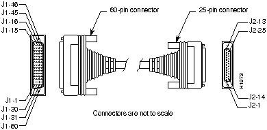
Table C-8 : EIA/TIA-232 DTE Cable Pinouts (DB-60 to DB-25)
| 60 Pin | Signal | Description | Direction | 25 Pin | Signal |
|---|---|---|---|---|---|
| J1-50
J1-51 J1-52 |
MODE_0
GND MODE_DCE |
Shorting group | -- | -- | -- |
| J1-46 | Shield GND | Single | -- | J2-1 | Shield GND |
| J1-41
Shield |
TxD/RxD
-- |
Twisted pair no. 5 | --->
-- |
J2-2
Shield |
TxD
-- |
| J1-36
Shield |
RxD/TxD
-- |
Twisted pair no. 9 | <---
-- |
J2-3
Shield |
RxD
-- |
| J1-42
Shield |
RTS/CTS
-- |
Twisted pair no. 4 | --->
-- |
J2-4
Shield |
RTS
-- |
| J1-35
Shield |
CTS/RTS
-- |
Twisted pair no. 10 | <---
-- |
J2-5
Shield |
CTS
-- |
| J1-34
Shield |
DSR/DTR
-- |
Twisted pair no. 11 | <---
-- |
J2-6
Shield |
DSR
-- |
| J1-45
Shield |
Circuit GND
-- |
Twisted pair no. 1 | --
-- |
J2-7
Shield |
Circuit GND
-- |
| J1-33
Shield |
DCD/LL
-- |
Twisted pair no. 12 | <---
-- |
J2-8
Shield |
DCD
-- |
| J1-37
Shield |
TxC/NIL
-- |
Twisted pair no. 8 | <---
-- |
J2-15
Shield |
TxC
-- |
| J1-38
Shield |
RxC/TxCE
-- |
Twisted pair no. 7 | <---
-- |
J2-17
Shield |
RxC
-- |
| J1-44
Shield |
LL/DCD
-- |
Twisted pair no. 2 | --->
-- |
J2-18
Shield |
LTST
-- |
| J1-43
Shield |
DTR/DSR
-- |
Twisted pair no. 3 | --->
-- |
J2-20
Shield |
DTR
-- |
| J1-39
Shield |
TxCE/TxC
-- |
Twisted pair no. 6 | --->
-- |
J2-24
Shield |
TxCE
-- |
Table C-9 : EIA/TIA-232 DCE Cable Pinouts (DB-60 to DB-25)
| 60 Pin | Signal | Description | Direction | 25 Pin | Signal |
|---|---|---|---|---|---|
| J1-50
J1-51 |
MODE_0
GND |
Shorting group | --
|
--
|
--
|
| J1-46 | Shield GND | Single | -- | J2-1 | Shield GND |
| J1-36
Shield |
RxD/TxD
-- |
Twisted pair no. 9 | <---
-- |
J2-2
Shield |
TxD
-- |
| J1-41
Shield |
TxD/RxD
-- |
Twisted pair no. 5 | --->
-- |
J2-3
Shield |
RxD
-- |
| J1-35
Shield |
CTS/RTS
-- |
Twisted pair no. 10 | <---
-- |
J2-4
Shield |
RTS
-- |
| J1-42
Shield |
RTS/CTS
-- |
Twisted pair no. 4 | --->
-- |
J2-5
Shield |
CTS
-- |
| J1-43
Shield |
DTR/DSR
-- |
Twisted pair no. 3 | --->
-- |
J2-6
Shield |
DSR
-- |
| J1-45
Shield |
Circuit GND
-- |
Twisted pair no. 1 | --
-- |
J2-7
Shield |
Circuit GND |
| J1-44
Shield |
LL/DCD
-- |
Twisted pair no. 2 | --->
-- |
J2-8
Shield |
DCD
-- |
| J1-39
Shield |
TxCE/TxC
-- |
Twisted pair no. 7 | --->
-- |
J2-15
Shield |
TxC
-- |
| J1-40
Shield |
NIL/RxC
-- |
Twisted pair no. 6 | --->
-- |
J2-17
Shield |
RxC
-- |
| J1-33
Shield |
DCD/LL
-- |
Twisted pair no. 12 | <---
-- |
J2-18
Shield |
LTST
-- |
| J1-34
Shield |
DSR/DTR
-- |
Twisted pair no. 11 | <---
-- |
J2-20
Shield |
DTR
-- |
| J1-38
Shield |
RxC/TxCE
-- |
Twisted pair no. 8 | <---
-- |
J2-24
Shield |
TxCE
-- |
Figure C-12 shows the EIA/TIA-449 cable assembly. Table C-10 lists the DTE pinouts. Table C-11 lists the DCE pinouts. Arrows indicate signal direction: a right arrow (--->) indicates DTE to DCE, and a left arrow (<---) indicates DCE to DTE.
Figure C-12 : EIA/TIA-449 Cable Assembly
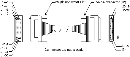
Table C-10 : EIA/TIA-449 DTE Cable Pinouts (DB-60 to DB-37)
| 60 Pin | Signal | Description | Direction | 37 Pin | Signal |
|---|---|---|---|---|---|
| J1-49
J1-48 |
MODE_1
GND |
Shorting group | -- | -- | -- |
| J1-51
J1-52 |
GND
MODE_DCE |
Shorting group | -- | -- | -- |
| J1-46 | Shield_GND | Single | _ | J2-1 | Shield GND |
| J1-11
J1-12 |
TxD/RxD+
TxD/RxD-- |
Twisted pair no. 6 | --->
---> |
J2-4
J2-22 |
SD+
SD-- |
| J1-24
J1-23 |
TxC/RxC+
TxC/RxC-- |
Twisted pair no. 9 | <---
<--- |
J2-5
J2-23 |
ST+
ST-- |
| J1-28
J1-27 |
RxD/TxD+
RxD/TxD-- |
Twisted pair no. 11 | <---
<--- |
J2-6
J2-24 |
RD+
RD-- |
| J1-9
J1-10 |
RTS/CTS+
RTS/CTS-- |
Twisted pair no. 5 | --->
---> |
J2-7
J2-25 |
RS+
RS-- |
| J1-26
J1-25 |
RxC/TxCE+
RxC/TxCE-- |
Twisted pair no. 10 | <---
<--- |
J2-8
J2-26 |
RT+
RT-- |
| J1-1
J1-2 |
CTS/RTS+
CTS/RTS-- |
Twisted pair no. 1 | <---
<--- |
J2-9
J2-27 |
CS+
CS-- |
| J1-44
J1-45 |
LL/DCD
Circuit_GND |
Twisted pair no. 12 | --->
_ |
J2-10
J2-37 |
LL
SC |
| J1-3
J1-4 |
DSR/DTR+
DSR/DTR-- |
Twisted pair no. 2 | <---
<--- |
J2-11
J2-29 |
DM+
DM-- |
| J1-7
J1-8 |
DTR/DSR+
DTR/DSR-- |
Twisted pair no. 4 | --->
---> |
J2-12
J2-30 |
TR+
TR-- |
| J1-5
J1-6 |
DCD/DCD+
DCD/DCD-- |
Twisted pair no. 3 | <---
<--- |
J2-13
J2-31 |
RR+
RR-- |
| J1-13
J1-14 |
TxCE/TxC+
TxCE/TxC-- |
Twisted pair no. 7 | --->
---> |
J2-17
J2-35 |
TT+
TT-- |
| J1-15
J1-16 |
Circuit_GND
Circuit_GND |
Twisted pair no. 9 | --
-- |
J2-19
J2-20 |
SG
RC |
Table C-11 : EIA/TIA-449 DCE Cable Pinouts (DB-60 to DB-37)
| 60 Pin | Signal | Description | Direction | 37 Pin | Signal |
|---|---|---|---|---|---|
| J1-49
J1-48 |
MODE_1
GND |
Shorting group | -- | -- | -- |
| J1-46 | Shield_GND | Single | -- | J2-1 | Shield GND |
| J1-28
J1-27 |
RxD/TxD+
RxD/TxD-- |
Twisted pair no. 11 | <---
<--- |
J2-4
J2-22 |
SD+
SD-- |
| J1-13
J1-14 |
TxCE/TxC+
TxCE/TxC-- |
Twisted pair no. 7 | --->
---> |
J2-5
J2-23 |
ST+
ST-- |
| J1-11
J1-12 |
TxD/RxD+
TxD/RxD-- |
Twisted pair no. 6 | --->
---> |
J2-6
J2-24 |
RD+
RD-- |
| J1-1
J1-2 |
CTS/RTS+
CTS/RTS-- |
Twisted pair no. 1 | <---
<--- |
J2-7
J2-25 |
RS+
RS-- |
| J1-24
J1-23 |
TxC/RxC+
TxC/RxC-- |
Twisted pair no. 9 | --->
---> |
J2-8
J2-26 |
RT+
RT-- |
| J1-9
J1-10 |
RTS/CTS+
RTS/CTS-- |
Twisted pair no. 5 | --->
---> |
J2-9
J2-27 |
CS+
CS-- |
| J1-29
J1-30 |
NIL/LL
Circuit_GND |
Twisted pair no. 12 | --->
-- |
J2-10
J2-37 |
LL
SC |
| J1-7
J1-8 |
DTR/DSR+
DTR/DSR-- |
Twisted pair no. 4 | --->
---> |
J2-11
J2-29 |
DM+
DM-- |
| J1-3
J1-4 |
DSR/DTR+
DSR/DTR-- |
Twisted pair no. 2 | <---
<--- |
J2-12
J2-30 |
TR+
TR-- |
| J1-5
J1-6 |
DCD/DCD+
DCD/DCD-- |
Twisted pair no. 3 | --->
---> |
J2-13
J2-31 |
RR+
RR-- |
| J1-26
J1-25 |
RxC/TxCE+
RxC/TxCE-- |
Twisted pair no. 10 | <---
<--- |
J2-17
J2-35 |
TT+
TT-- |
| J1-15
J1-16 |
Circuit_GND
Circuit_GND |
Twisted pair no. 8 | _
_ |
J2-19
J2-20 |
SG
RC |
Figure C-13 shows the V.35 cable assembly. Table C-12 lists the DTE pinouts. Table C-13 lists the DCE pinouts. Arrows indicate signal direction: a right arrow (--->) indicates DTE to DCE, and a left arrow (<---) indicates DCE to DTE.
Figure C-13 : V.35 Cable Assembly
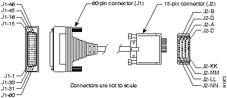
Table C-12 : V.35 DTE Cable Pinouts (DB-60 to 34-Pin)
| 60 Pin | Signal | Description | Direction | 34 Pin | Signal |
|---|---|---|---|---|---|
| J1-49
J1-48 |
MODE_1
GND |
Shorting group | -- | -- | -- |
| J1-50
J1-51 J1-52 |
MODE_0
GND MODE_DCE |
Shorting group | -- | -- | -- |
| J1-53
J1-54 J1-55 J1-56 |
TxC/NIL
RxC_TxCE RxD/TxD GND |
Shorting group | -- | -- | -- |
| J1-46 | Shield_GND | Single | -- | J2-A | Frame GND |
| J1-45
Shield |
Circuit_GND
-- |
Twisted pair no. 12 | --
-- |
J2-B
Shield |
Circuit GND
-- |
| J1-42
Shield |
RTS/CTS
-- |
Twisted pair no. 9 | --->
-- |
J2-C
Shield |
RTS
-- |
| J1-35
Shield |
CTS/RTS
-- |
Twisted pair no. 8 | <---
-- |
J2-D
Shield |
CTS
-- |
| J1-34
Shield |
DSR/DTR
-- |
Twisted pair no. 7 | <---
-- |
J2-E
Shield |
DSR
-- |
| J1-33
Shield |
DCD/LL
-- |
Twisted pair no. 6 | <---
-- |
J2-F
Shield |
RLSD
-- |
| J1-43
Shield |
DTR/DSR
-- |
Twisted pair no. 10 | --->
-- |
J2-H
Shield |
DTR
-- |
| J1-44
Shield |
LL/DCD
-- |
Twisted pair no. 11 | --->
-- |
J2-K
Shield |
LT
-- |
| J1-18
J1-17 |
TxD/RxD+
TxD/RxD-- |
Twisted pair no. 1 | --->
---> |
J2-P
J2-S |
SD+
SD-- |
| J1-28
J1-27 |
RxD/TxD+
RxD/TxD-- |
Twisted pair no. 5 | <---
<--- |
J2-R
J2-T |
RD+
RD-- |
| J1-20
J1-19 |
TxCE/TxC+
TxCE/TxC-- |
Twisted pair no. 2 | --->
---> |
J2-U
J2-W |
SCTE+
SCTE-- |
| J1-26
J1-25 |
RxC/TxCE+
RxC/TxCE-- |
Twisted pair no. 4 | <---
<--- |
J2-V
J2-X |
SCR+
SCR-- |
| J1-24
J1-23 |
TxC/RxC+
TxC/RxC-- |
Twisted pair no. 3 | <---
<--- |
J2-Y
J2-AA |
SCT+
SCT-- |
Table C-13 : V.35 DCE Cable Pinouts (DB-60 to 34-Pin)
| 60 Pin | Signal | Description | Direction | 34 Pin | Signal |
|---|---|---|---|---|---|
| J1-49
J1-48 |
MODE_1
GND |
Shorting group | -- | -- | -- |
| J1-50
J1-51 |
MODE_0
GND |
Shorting group | -- | -- | -- |
| J1-53
J1-54 J1-55 J1-56 |
TxC/NIL
RxC_TxCE RxD/TxD GND |
Shorting group | -- | -- | -- |
| J1-46 | Shield_GND | Single | -- | J2-A | Frame GND |
| J1-45
Shield |
Circuit_GND
-- |
Twisted pair no. 12 | --
-- |
J2-B
Shield |
Circuit GND
-- |
| J1-35
Shield |
CTS/RTS
-- |
Twisted pair no. 8 | <---
-- |
J2-C
Shield |
RTS
-- |
| J1-42
Shield |
RTS/CTS
-- |
Twisted pair no. 9 | --->
-- |
J2-D
Shield |
CTS
-- |
| J1-43
Shield |
DTR/DSR
-- |
Twisted pair no. 10 | --->
-- |
J2-E
Shield |
DSR
-- |
| J1-44
Shield |
LL/DCD
-- |
Twisted pair no. 11 | --->
-- |
J2-F
Shield |
RLSD
-- |
| J1-34
Shield |
DSR/DTR
-- |
Twisted pair no. 7 | <---
-- |
J2-H
Shield |
DTR
-- |
| J1-33
Shield |
DCD/LL
-- |
Twisted pair no. 6 | <---
-- |
J2-K
Shield |
LT
-- |
| J1-28
J1-27 |
RxD/TxD+
RxD/TxD-- |
Twisted pair no. 5 | <---
<--- |
J2-P
J2-S |
SD+
SD-- |
| J1-18
J1-17 |
TxD/RxD+
TxD/RxD-- |
Twisted pair no. 1 | --->
---> |
J2-R
J2-T |
RD+
RD-- |
| J1-26
J1-25 |
RxC/TxCE+
RxC/TxCE-- |
Twisted pair no. 4 | <---
<--- |
J2-U
J2-W |
SCTE+
SCTE-- |
| J1-22
J1-21 |
NIL/RxC+
NIL/RxC-- |
Twisted pair no. 3 | --->
---> |
J2-V
J2-X |
SCR+
SCR-- |
| J1-20
J1-19 |
TxCE/TxC+
TxCE/TxC-- |
Twisted pair no. 2 | --->
---> |
J2-Y
J2-AA |
SCT+
SCT-- |
Figure C-14 shows the X.21 cable assembly. Table C-14 lists the DTE pinouts. Table C-15 lists the DCE pinouts. Arrows indicate signal direction: a right arrow (--->) indicates DTE to DCE, and a left arrow (<---) indicates DCE to DTE.
Figure C-14 : X.21 Cable Assembly
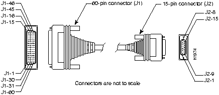
Table C-14 : X.21 DTE Cable Pinouts (DB-60 to DB-15)
| 60 Pin | Signal | Description | Direction | 15 Pin | Signal |
|---|---|---|---|---|---|
| J1-48
J1-47 |
GND
MODE_2 |
Shorting group | -- | -- | -- |
| J1-51
J1-52 |
GND
MODE_DCE |
Shorting group | -- | -- | -- |
| J1-46 | Shield_GND | Single | -- | J2-1 | Shield GND |
| J1-11
J1-12 |
TxD/RxD+
TxD/RxD-- |
Twisted pair no. 3 | --->
---> |
J2-2
J2-9 |
Transmit+
Transmit-- |
| J1-9
J1-10 |
RTS/CTS+
RTS/CTS-- |
Twisted pair no. 2 | --->
---> |
J2-3
J2-10 |
Control+
Control-- |
| J1-28
J1-27 |
RxD/TxD+
RxD/TxD-- |
Twisted pair no. 6 | <---
<--- |
J2-4
J2-11 |
Receive+
Receive-- |
| J1-1
J1-2 |
CTS/RTS+
CTS/RTS-- |
Twisted pair no. 1 | <---
<--- |
J2-5
J2-12 |
Indication+
Indication-- |
| J1-26
J1-25 |
RxC/TxCE+
RxC/TxCE-- |
Twisted pair no. 5 | <---
<--- |
J2-6
J2-13 |
Timing+
Timing-- |
| J1-15
Shield |
Control_GND
-- |
Twisted pair no. 4 | --
-- |
J2-8
Shield |
Control GND
-- |
Table C-15 : X.21 DCE Cable Pinouts (DB-60 to DB-15)
| 60 Pin | Signal | Description | Direction | 15 Pin | Signal |
|---|---|---|---|---|---|
| J1-48
J1-47 |
GND
MODE_2 |
Shorting group | -- | -- | -- |
| J1-46 | Shield_GND | Single | -- | J2-1 | Shield GND |
| J1-28
J1-27 |
RxD/TxD+
RxD/TxD-- |
Twisted pair no. 6 | <---
<--- |
J2-2
J2-9 |
Transmit+
Transmit-- |
| J1-1
J1-2 |
CTS/RTS+
CTS/RTS-- |
Twisted pair no. 1 | <---
<--- |
J2-3
J2-10 |
Control+
Control-- |
| J1-11
J1-12 |
TxD/RxD+
TxD/RxD-- |
Twisted pair no. 3 | --->
---> |
J2-4
J2-11 |
Receive+
Receive-- |
| J1-9
J1-10 |
RTS/CTS+
RTS/CTS-- |
Twisted pair no. 2 | --->
---> |
J2-5
J2-12 |
Indication+
Indication-- |
| J1-24
J1-23 |
TxC/RxC+
TxC/RxC-- |
Twisted pair no. 4 | --->
---> |
J2-6
J2-13 |
Timing+
Timing-- |
| J1-15
Shield |
Control_GND
-- |
Twisted pair no. 5 | --
-- |
J2-8
Shield |
Control GND
-- |
Alarm Cable Assembly and Pinouts
Table C-16 lists the pinouts for the alarm port.
Table C-16 : Alarm Port Pinouts
| Pin | Description |
|---|---|
| 1 | Normally open |
| 2 | Common |
| 3 | Normally closed |
|
|
Copyright 1988-1996 © Cisco Systems Inc.