|
|

The AS51 network application card (NAC) console port is configured as data communications equipment (DCE), and the auxiliary port is configured as data terminal equipment (DTE). The console and auxiliary ports both use RJ-45 connectors. RJ-45-to-DB-25 adapters are available for connection to modems and other external communications equipment. Both ports are configured as asynchronous serial ports.
Following are the pinouts for the console port (see Table B-1), the auxiliary port (see Table B-2), and the RJ-45 Ethernet port (see Table B-3).
Table B-1 AS51 NAC Console Port Pinouts (RJ-45-to-DB-25 Female)
| Console Port (DCE) | RJ-45-to-DB-25 Adapter | ||||
|---|---|---|---|---|---|
| Pin(1) | Signal | Input/Output | RJ-45 Pin | Signal | DB-25 Pin |
| 1 | -- | -- | 1 | CTS | 4 |
| 2 | CD | Output | 2 | DSR | 20 |
| 3 | RxD | Output | 3 | RxD | 2 |
| 4 | GND | -- | 4 | GND | 7 |
| 5 | GND | -- | 5 | GND | 7 |
| 6 | TxD | Input | 6 | TxD | 3 |
| 7 | DTR | Input | 7 | DTR | 6 |
| 8 | -- | -- | 8 | RTS | 5 |
Table B-2 Access Server NAC Auxiliary Port Pinouts (RJ-45-to-DB-25 Male)
| Auxiliary Port (DTE) | RJ-45 to DB-25 Adapter | ||||
|---|---|---|---|---|---|
| Pin(1) | Signal | Input/Output | RJ-45 Pin | Signal | DB-25 Pin |
| 1 | CTS | Input | 1 | CTS | 5 |
| 2 | CD/RING | Input | 2 | DSR | 6 |
| 3 | RxD | Input | 3 | RxD | 3 |
| 4 | GND | -- | 4 | GND | 7 |
| 5 | GND | -- | 5 | GND | 7 |
| 6 | TxD | Output | 6 | TxD | 2 |
| 7 | DTR | Output | 7 | DTR | 20 |
| 8 | RTS | Output | 8 | RTS | 4 |
Table B-3 Access Server NAC RJ-45 Ethernet Port Pinouts
| Pin(1) | IEEE Name | Description |
|---|---|---|
| 1 | TD+ | Transmit data + |
| 2 | TD-- | Transmit data -- |
| 3 | RD+ | Receive data + |
| 4 | Not used | |
| 5 | Not used | |
| 6 | RD-- | Receive data -- |
| 7 | Not used | |
| 8 | Not used |
Figure B-1 shows the asynchronous serial interface DB-50 breakout cable assembly, and Table B-4 contains the pinout information. The breakout cable is used to connect one asynchronous serial port on an AS51 network interface card (NIC) to serial ports on two quad modem NICs.
Figure B-1 Asynchronous Serial Interface DB-50 Breakout Cable Assembly
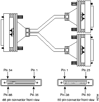
Table B-4 68-Pin SCSI to Dual DB-50 Breakout Cable Pinouts
| Signal | HD-68Pin | ---> |
HD-50 Cable 1 Pin | HD-50 Cable 2 Pin |
Signal | HD-68Pin | ---> |
HD-50 Cable 1 Pin | HD-50 Cable 2 Pin |
|
|---|---|---|---|---|---|---|---|---|---|---|
| DGND | 1 | 7 | -- | DGND | 35(1) | -- | -- | |||
| RTS0 | 2 | 3 | -- | DTR0 | 36 | 5 | -- | |||
| TXD0 | 3 | 1 | -- | DGND | 37 | 19 | -- | |||
| -- | 4 | -- | -- | RXD0 | 38 | 2 | -- | |||
| DSR0 | 5 | 6 | -- | CTS0 | 39 | 4 | -- | |||
| RTS1 | 6 | 28 | -- | DTR1 | 40 | 30 | -- | |||
| TXD1 | 7 | 26 | -- | DGND | 41 | 32 | -- | |||
| -- | 8 | -- | -- | RXD1 | 42 | 27 | -- | |||
| DSR1 | 9 | 31 | -- | CTS1 | 43 | 29 | -- | |||
| RTS2 | 10 | 40 | -- | DTR2 | 44 | 42 | -- | |||
| TXD2 | 11 | 38 | -- | DGND | 45 | 44 | -- | |||
| 12 | -- | -- | RXD2 | 46 | 39 | -- | ||||
| DSR2 | 13 | 43 | -- | CTS2 | 47 | 41 | -- | |||
| RTS3 | 14 | 15 | -- | DTR3 | 48 | 17 | -- | |||
| TXD3 | 15 | 13 | -- | DGND | 49 | -- | 7 | |||
| 16 | -- | -- | RXD3 | 50 | 14 | -- | ||||
| DSR3 | 17 | 18 | -- | CTS3 | 51 | 16 | -- | |||
| RTS4 | 18 | -- | 3 | DTR4 | 52 | -- | 5 | |||
| TXD4 | 19 | -- | 1 | DGND | 53 | -- | 19 | |||
| 20 | -- | -- | RXD4 | 54 | -- | 2 | ||||
| DSR4 | 21 | -- | 6 | CTS4 | 55 | -- | 4 | |||
| RTS5 | 22 | -- | 28 | DTR5 | 56 | -- | 30 | |||
| TXD5 | 23 | -- | 26 | DGND | 57 | -- | 32 | |||
| 24 | -- | -- | RXD5 | 58 | -- | 27 | ||||
| DSR5 | 25 | -- | 31 | CTS5 | 59 | -- | 29 | |||
| RTS6 | 26 | -- | 40 | DTR6 | 60 | -- | 42 | |||
| TXD6 | 27 | -- | 38 | DGND | 61 | -- | 44 | |||
| 28 | -- | -- | RXD6 | 62 | -- | 39 | ||||
| DSR6 | 29 | -- | 43 | CTS6 | 63 | -- | 41 | |||
| RTS7 | 30 | -- | 15 | DTR7 | 64 | -- | 17 | |||
| TXD7 | 31 | -- | 13 | DGND | 65 | -- | 25 | |||
| 32 | -- | -- | RXD7 | 66 | -- | 14 | ||||
| DSR7 | 33 | -- | 18 | CTS7 | 67 | -- | 16 | |||
| CABLE | 341 | -- | -- | CGND | 68 | 50 | -- |
The illustrations and tables in this section provide assembly drawings and pinout for the EIA/TIA-530 DTE, EIA/TIA-232, EIA/TIA-449, V.35, and X.21 DTE and DCE cables, and the synchronous serial interface port pinouts.
Figure B-2 shows the EIA/TIA-530 DTE cable assembly. Table B-5 lists the EIA/TIA-530 DTE cable pinouts. Arrows indicate signal direction: ---> indicates DTE to DCE, and <--- indicates DCE to DTE.
Figure B-2 EIA/TIA-530 DTE Cable Assembly
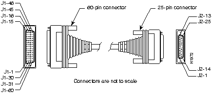
Table B-5 EIA-530 DTE Male Cable Pinout (DB-60 to DB-25)
| 60 Pin(1) | Signal | 25 Pin | Signal | DirectionDTE DCE |
|---|---|---|---|---|
| J1-1J1-2 | CTS/RTS+CTS/RTS-- | J2-5J2-13 | CB(A), CTS+ CB(B), CTS-- | <---<--- |
| J1-3J1-4 | DSR/DTR+DSR/DTR-- | J2-6J2-22 | CC(A), DSR+ CC(B), DSR-- | <---<--- |
| J1-5J1-6 | DCD/DCD+DCD/DCD-- | J2-8J2-10 | CF(A), DCD+CF(B), DCD-- | <---<--- |
| J1-7J1-8 | DTR/DSR+DTR/DSR-- | J2-20J2-23 | CD(A), DTR+CD(B), DTR-- | --->---> |
| J1-9J1-10 | RTS/CTS+RTS/CTS-- | J2-4J2-19 | CA(A), RTS+CA(B), RTS-- | --->---> |
| J1-11J1-12 | TxD/RxD+TxD/RxD-- | J2-2J2-14 | BA(A), TxD+BA(B), TxD-- | --->---> |
| J1-13J1-14 | TxCE/TxC+TxCE/TxC-- | J2-24J2-11 | DA(A), TxCE+DA(B), TxCE-- | --->---> |
| J1-24J1-23 | TxC/RxC+TxC/RxC-- | J2-15J2-12 | DB(A), TxC+DB(B), TxC-- | <---<--- |
| J1-26J1-25 | RxC/TxCE+RxC/TxCE-- | J2-17J2-9 | DD(A), RxC+DD(B), RxC-- | <---<--- |
| J1-28J1-27 | RxD/TxD+RxD/TxD-- | J2-3J2-16 | BB(A), RxD+BB(B), RxD-- | <---<--- |
| J1-44J1-45 | LL/DCDCircuit_GND | J2-18J2-7 | LL Circuit_ GND | --->-- |
| J1-46J1-47 | Shield_GNDMODE_2 | J2-1-- | Shield-- | Shorted |
| J1-48J1-49 | GNDMODE_1 | ---- | ---- | Shorted |
| J1-51J1-52 | GNDMODE_DCE | ---- | ---- | Shorted |
Figure B-3 shows the EIA/TIA-232 cable assembly. Table B-6 lists the EIA/TIA-232 DTE pinout; and Table B-7 lists the EIA/TIA-232 DCE pinout. Arrows indicate signal direction: ---> indicates DTE to DCE, and <--- indicates DCE to DTE.
Figure B-3 EIA/TIA-232 Cable Assembly
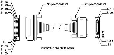
Table B-6 EIA/TIA-232 DTE Male Cable Pinout (DB-60-to-DB-25)
| 60 Pin(1) | Signal | Description | Direction | 25 Pin | Signal |
|---|---|---|---|---|---|
| J1-50J1-51J1-52 | MODE_0GNDMODE_DCE | Shorting group | -- | -- | -- |
| J1-46 | Shield GND | Single | -- | J2-1 | Shield GND |
| J1-41Shield | TxD/RxD-- | Twisted pair no. 5 | --->-- | J2-2Shield | TxD-- |
| J1-36Shield | RxD/TxD-- | Twisted pair no. 9 | <----- | J2-3Shield | RxD-- |
| J1-42Shield | RTS/CTS-- | Twisted pair no. 4 | --->-- | J2-4Shield | RTS-- |
| J1-35Shield | CTS/RTS-- | Twisted pair no. 10 | <----- | J2-5Shield | CTS-- |
| J1-34Shield | DSR/DTR-- | Twisted pair no. 11 | <----- | J2-6Shield | DSR-- |
| J1-45Shield | Circuit GND-- | Twisted pair no. 1 | ---- | J2-7Shield | Circuit GND-- |
| J1-33Shield | DCD/LL-- | Twisted pair no. 12 | <----- | J2-8Shield | DCD-- |
| J1-37Shield | TxC/NIL-- | Twisted pair no. 8 | <----- | J2-15Shield | TxC-- |
| J1-38Shield | RxC/TxCE-- | Twisted pair no. 7 | <----- | J2-17Shield | RxC-- |
| J1-44Shield | LL/DCD-- | Twisted pair no. 2 | --->-- | J2-18Shield | LTST-- |
| J1-43Shield | DTR/DSR-- | Twisted pair no. 3 | --->-- | J2-20Shield | DTR-- |
| J1-39Shield | TxCE/TxC-- | Twisted pair no. 6 | --->-- | J2-24Shield | TxCE-- |
Table B-7 EIA/TIA-232 DCE Female Cable Pinout (DB-60-to-DB-25)
| 60 Pin(1) | Signal | Description | Direction | 25 Pin | Signal |
|---|---|---|---|---|---|
| J1-50J1-51 | MODE_0GND | Shorting Group | -- |
-- |
-- |
| J1-46 | Shield GND | Single | -- | J2-1 | Shield GND |
| J1-36Shield | RxD/TxD-- | Twisted pair no. 9 | <----- | J2-2Shield | TxD-- |
| J1-41Shield | TxD/RxD-- | Twisted pair no. 5 | --->-- | J2-3Shield | RxD-- |
| J1-35Shield | CTS/RTS-- | Twisted pair no. 10 | <----- | J2-4Shield | RTS-- |
| J1-42Shield | RTS/CTS-- | Twisted pair no. 4 | --->-- | J2-5Shield | CTS-- |
| J1-43Shield | DTR/DSR-- | Twisted pair no. 3 | --->-- | J2-6Shield | DSR-- |
| J1-45Shield | Circuit GND-- | Twisted pair no. 1 | ---- | J2-7Shield | Circuit GND |
| J1-44Shield | LL/DCD-- | Twisted pair no. 2 | --->-- | J2-8Shield | DCD-- |
| J1-39Shield | TxCE/TxC-- | Twisted pair no. 7 | --->-- | J2-15Shield | TxC-- |
| J1-40Shield | NIL/RxC-- | Twisted pair no. 6 | --->-- | J2-17Shield | RxC-- |
| J1-33Shield | DCD/LL-- | Twisted pair no. 12 | <----- | J2-18Shield | LTST-- |
| J1-34Shield | DSR/DTR-- | Twisted pair no. 11 | <----- | J2-20Shield | DTR-- |
| J1-38Shield | RxC/TxCE-- | Twisted pair no. 8 | <----- | J2-24Shield | TxCE-- |
Figure B-4 shows the EIA/TIA-449 cable assembly. Table B-8 lists the EIA/TIA-449 DTE pinout, and Table B-9 lists the EIA/TIA-449 cable assembly DCE pinout. Arrows indicate signal direction: ---> indicates DTE to DCE, and <--- indicates DCE to DTE.
Figure B-4 EIA/TIA-449 Cable Assembly
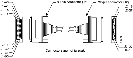
Table B-8 EIA/TIA-449 DTE Male Cable Pinout (DB-60-to-DB-37)
| 60 Pin(1) | Signal | Description | Direction | 37 Pin | Signal |
|---|---|---|---|---|---|
| J1-49J1-48 | MODE_1GND | Shorting group | -- | -- | -- |
| J1-51J1-52 | GNDMODE_DCE | Shorting group | -- | -- | -- |
| J1-46 | Shield_GND | Single | _ | J2-1 | Shield GND |
| J1-11J1-12 | TxD/RxD+TxD/RxD-- | Twisted pair no. 6 | --->---> | J2-4J2-22 | SD+SD-- |
| J1-24J1-23 | TxC/RxC+TxC/RxC-- | Twisted pair no. 9 | <---<--- | J2-5J2-23 | ST+ST-- |
| J1-28J1-27 | RxD/TxD+RxD/TxD-- | Twisted pair no. 11 | <---<--- | J2-6J2-24 | RD+RD-- |
| J1-9J1-10 | RTS/CTS+RTS/CTS-- | Twisted pair no. 5 | --->---> | J2-7J2-25 | RS+RS-- |
| J1-26J1-25 | RxC/TxCE+RxC/TxCE-- | Twisted pair no. 10 | <---<--- | J2-8J2-26 | RT+RT-- |
| J1-1J1-2 | CTS/RTS+CTS/RTS-- | Twisted pair no. 1 | <---<--- | J2-9J2-27 | CS+CS-- |
| J1-44J1-45 | LL/DCDCircuit_GND | Twisted pair no. 12 | --->_ | J2-10J2-37 | LLSC |
| J1-3J1-4 | DSR/DTR+DSR/DTR-- | Twisted pair no. 2 | <---<--- | J2-11J2-29 | DM+DM-- |
| J1-7J1-8 | DTR/DSR+DTR/DSR-- | Twisted pair no. 4 | --->---> | J2-12J2-30 | TR+TR-- |
| J1-5J1-6 | DCD/DCD+DCD/DCD-- | Twisted pair no. 3 | <---<--- | J2-13J2-31 | RR+RR-- |
| J1-13J1-14 | TxCE/TxC+TxCE/TxC-- | Twisted pair no. 7 | --->---> | J2-17J2-35 | TT+TT-- |
| J1-15J1-16 | Circuit_GNDCircuit_GND | Twisted pair no. 9 | ---- | J2-19J2-20 | SGRC |
Table B-9 EIA/TIA-449 DCE Female Cable Pinout (DB-60-to-DB-37)
| 60 Pin(1) | Signal | Description | Direction | 37 Pin | Signal |
|---|---|---|---|---|---|
| J1-49J1-48 | MODE_1GND | Shorting group | -- | -- | -- |
| J1-46 | Shield_GND | Single | -- | J2-1 | Shield GND |
| J1-28J1-27 | RxD/TxD+RxD/TxD-- | Twisted pair no. 11 | <---<--- | J2-4J2-22 | SD+SD-- |
| J1-13J1-14 | TxCE/TxC+TxCE/TxC-- | Twisted pair no. 7 | --->---> | J2-5J2-23 | ST+ST-- |
| J1-11J1-12 | TxD/RxD+TxD/RxD-- | Twisted pair no. 6 | --->---> | J2-6J2-24 | RD+RD-- |
| J1-1J1-2 | CTS/RTS+CTS/RTS-- | Twisted pair no. 1 | <---<--- | J2-7J2-25 | RS+RS-- |
| J1-24J1-23 | TxC/RxC+TxC/RxC-- | Twisted pair no. 9 | --->---> | J2-8J2-26 | RT+RT-- |
| J1-9J1-10 | RTS/CTS+RTS/CTS-- | Twisted pair no. 5 | --->---> | J2-9J2-27 | CS+CS-- |
| J1-29J1-30 | NIL/LLCircuit_GND | Twisted pair no. 12 | --->-- | J2-10J2-37 | LLSC |
| J1-7J1-8 | DTR/DSR+DTR/DSR-- | Twisted pair no. 4 | --->---> | J2-11J2-29 | DM+DM-- |
| J1-3J1-4 | DSR/DTR+DSR/DTR-- | Twisted pair no. 2 | <---<--- | J2-12J2-30 | TR+TR-- |
| J1-5J1-6 | DCD/DCD+DCD/DCD-- | Twisted pair no. 3 | --->---> | J2-13J2-31 | RR+RR-- |
| J1-26J1-25 | RxC/TxCE+RxC/TxCE-- | Twisted pair no. 10 | <---<--- | J2-17J2-35 | TT+TT-- |
| J1-15J1-16 | Circuit_GNDCircuit_GND | Twisted pair no. 8 | __ | J2-19J2-20 | SGRC |
Figure B-5 shows the V.35 cable assembly. Table B-10 lists the V.35 DTE cable pinout, and Table B-11 lists the V.35 DCE cable pinout. Arrows indicate signal direction: ---> indicates DTE to DCE, and <--- indicates DCE to DTE.
Figure B-5 V.35 Cable Assembly
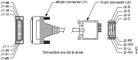
Table B-10 V.35 DTE Male Cable Pinout (DB-60-to-34-Pin)
| 60 Pin(1) | Signal | Description | Direction | 34 Pin | Signal |
|---|---|---|---|---|---|
| J1-49J1-48 | MODE_1GND | Shorting group | -- | -- | -- |
| J1-50J1-51J1-52 | MODE_0GNDMODE_DCE | Shorting group | -- | -- | -- |
| J1-53J1-54J1-55J1-56 | TxC/NILRxC_TxCERxD/TxDGND | Shorting group | -- | -- | -- |
| J1-46 | Shield_GND | Single | -- | J2-A | Frame GND |
| J1-45Shield | Circuit_GND-- | Twisted pair no. 12 | ---- | J2-BShield | Circuit GND-- |
| J1-42Shield | RTS/CTS-- | Twisted pair no. 9 | --->-- | J2-CShield | RTS-- |
| J1-35Shield | CTS/RTS-- | Twisted pair no. 8 | <----- | J2-DShield | CTS-- |
| J1-34Shield | DSR/DTR-- | Twisted pair no. 7 | <----- | J2-EShield | DSR-- |
| J1-33Shield | DCD/LL-- | Twisted pair no. 6 | <----- | J2-FShield | RLSD-- |
| J1-43Shield | DTR/DSR-- | Twisted pair no. 10 | --->-- | J2-HShield | DTR-- |
| J1-44Shield | LL/DCD-- | Twisted pair no. 11 | --->-- | J2-KShield | LT-- |
| J1-18J1-17 | TxD/RxD+TxD/RxD-- | Twisted pair no. 1 | --->---> | J2-PJ2-S | SD+SD-- |
| J1-28J1-27 | RxD/TxD+RxD/TxD-- | Twisted pair no. 5 | <---<--- | J2-RJ2-T | RD+RD-- |
| J1-20J1-19 | TxCE/TxC+TxCE/TxC-- | Twisted pair no. 2 | --->---> | J2-UJ2-W | SCTE+SCTE-- |
| J1-26J1-25 | RxC/TxCE+RxC/TxCE-- | Twisted pair no. 4 | <---<--- | J2-VJ2-X | SCR+SCR-- |
| J1-24J1-23 | TxC/RxC+TxC/RxC-- | Twisted pair no. 3 | <---<--- | J2-YJ2-AA | SCT+SCT-- |
Table B-11 V.35 DCE Female Cable Pinout (DB-60-to-34-Pin)
| 60 Pin(1) | Signal | Description | Direction | 34 Pin | Signal |
|---|---|---|---|---|---|
| J1-49J1-48 | MODE_1GND | Shorting group | -- | -- | -- |
| J1-50J1-51 | MODE_0GND | Shorting Group | -- | -- | -- |
| J1-53J1-54J1-55J1-56 | TxC/NILRxC_TxCERxD/TxDGND | Shorting Group | -- | -- | -- |
| J1-46 | Shield_GND | Single | -- | J2-A | Frame GND |
| J1-45Shield | Circuit_GND-- | Twisted pair no. 12 | ---- | J2-BShield | Circuit GND-- |
| J1-35Shield | CTS/RTS-- | Twisted pair no. 8 | <----- | J2-CShield | RTS-- |
| J1-42Shield | RTS/CTS-- | Twisted pair no. 9 | --->-- | J2-DShield | CTS-- |
| J1-43Shield | DTR/DSR-- | Twisted pair no. 10 | --->-- | J2-EShield | DSR-- |
| J1-44Shield | LL/DCD-- | Twisted pair no. 11 | --->-- | J2-FShield | RLSD-- |
| J1-34Shield | DSR/DTR-- | Twisted pair no. 7 | <----- | J2-HShield | DTR-- |
| J1-33Shield | DCD/LL-- | Twisted pair no. 6 | <----- | J2-KShield | LT-- |
| J1-28J1-27 | RxD/TxD+RxD/TxD-- | Twisted pair no. 5 | <---<--- | J2-PJ2-S | SD+SD-- |
| J1-18J1-17 | TxD/RxD+TxD/RxD-- | Twisted pair no. 1 | --->---> | J2-RJ2-T | RD+RD-- |
| J1-26J1-25 | RxC/TxCE+RxC/TxCE-- | Twisted pair no. 4 | <---<--- | J2-UJ2-W | SCTE+SCTE-- |
| J1-22J1-21 | NIL/RxC+NIL/RxC-- | Twisted pair no. 3 | --->---> | J2-VJ2-X | SCR+SCR-- |
| J1-20J1-19 | TxCE/TxC+TxCE/TxC-- | Twisted pair no. 2 | --->---> | J2-YJ2-AA | SCT+SCT-- |
Figure B-6 shows the X.21 cable assembly. Table B-12 lists the X.21 DTE cable pinout, and Table B-13 lists the X.21 DCE cable pinout. Arrows indicate signal direction: ---> indicates DTE to DCE, and <--- indicates DCE to DTE.
Figure B-6 X.21 Cable Assembly
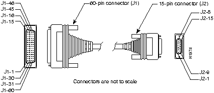
Table B-12 X.21 DTE Male Cable Pinout (DB-60-to-DB-15)
| 60 Pin(1) | Signal | Description | Direction | 15 Pin | Signal |
|---|---|---|---|---|---|
| J1-48J1-47 | GNDMODE_2 | Shorting group | - | -- | -- |
| J1-51J1-52 | GNDMODE_DCE | Shorting group | -- | -- | -- |
| J1-46 | Shield_GND | Single | -- | J2-1 | Shield GND |
| J1-11J1-12 | TxD/RxD+TxD/RxD-- | Twisted pair no. 3 | --->---> | J2-2J2-9 | Transmit+Transmit-- |
| J1-9J1-10 | RTS/CTS+RTS/CTS-- | Twisted pair no. 2 | --->---> | J2-3J2-10 | Control+Control-- |
| J1-28J1-27 | RxD/TxD+RxD/TxD-- | Twisted pair no. 6 | <---<--- | J2-4J2-11 | Receive+Receive-- |
| J1-1J1-2 | CTS/RTS+CTS/RTS-- | Twisted pair no. 1 | <---<--- | J2-5J2-12 | Indication+Indication-- |
| J1-26J1-25 | RxC/TxCE+RxC/TxCE-- | Twisted pair no. 5 | <---<--- | J2-6J2-13 | Timing+Timing-- |
| J1-15Shield | Control_GND-- | Twisted pair no. 4 | ---- | J2-8Shield | Control GND-- |
Table B-13 X.21 DCE Female Cable Pinout (DB-60-to-DB-15)
| 60 Pin(1) | Signal | Description | Direction | 15 Pin | Signal |
|---|---|---|---|---|---|
| J1-48J1-47 | GNDMODE_2 | Shorting group | -- | -- | -- |
| J1-46 | Shield_GND | Single | -- | J2-1 | Shield GND |
| J1-28J1-27 | RxD/TxD+RxD/TxD-- | Twisted pair no. 6 | <---<--- | J2-2J2-9 | Transmit+Transmit-- |
| J1-1J1-2 | CTS/RTS+CTS/RTS-- | Twisted pair no. 1 | <---<--- | J2-3J2-10 | Control+Control-- |
| J1-11J1-12 | TxD/RxD+TxD/RxD-- | Twisted pair no. 3 | --->---> | J2-4J2-11 | Receive+Receive-- |
| J1-9J1-10 | RTS/CTS+RTS/CTS-- | Twisted pair no. 2 | --->---> | J2-5J2-12 | Indication+Indication-- |
| J1-24J1-23 | TxC/RxC+TxC/RxC-- | Twisted pair no. 4 | --->---> | J2-6J2-13 | Timing+Timing-- |
| J1-15Shield | Control_GND-- | Twisted pair no. 5 | ---- | J2-8Shield | Control GND-- |
Table B-14 lists the pinouts for the DB-60 synchronous serial interface port.
Table B-14 Synchronous Serial Interface Port (DB-60)
| 60 Pin(1) | Signal | Description |
|---|---|---|
| J1-50J1-51J1-52 | MODE_0GNDMODE_DCE | Shorting group |
| J1-46 | Shield GND | Single |
| J1-41Shield | TxD/RxD-- | Twisted pair no. 5 |
| J1-36Shield | RxD/TxD-- | Twisted pair no. 9 |
| J1-42Shield | RTS/CTS-- | Twisted pair no. 4 |
| J1-35Shield | CTS/RTS-- | Twisted pair no. 10 |
| J1-34Shield | DSR/DTR-- | Twisted pair no. 11 |
| J1-45Shield | Circuit GND-- | Twisted pair no. 1 |
| J1-33Shield | DCD/LL-- | Twisted pair no. 12 |
| J1-37Shield | TxC/NIL-- | Twisted pair no. 8 |
| J1-38Shield | RxC/TxCE-- | Twisted pair no. 7 |
| J1-44Shield | LL/DCD-- | Twisted pair no. 2 |
| J1-43Shield | DTR/DSR-- | Twisted pair no. 3 |
| J1-39Shield | TxCE/TxC-- | Twisted pair no. 6 |
Table B-15 through Table B-19 list the pinouts for the network management NAC serial, 10BaseT, 10Base5, and 10Base2 ports and the UTP connector.
Table B-15 Network Management NAC Serial Port (DTE)
| 8-Position Modular Jack | Circuit | Function | Direction |
|---|---|---|---|
| 1 | CC | Data Set Ready | Inbound |
| 2 | CF | Carrier Detect | Inbound |
| 3 | CD | Data Terminal Ready | Outbound |
| 4 | AB | Signal Ground | -- |
| 5 | BB | Receive Data | Inbound |
| 6 | BA | Transmit Data | Outbound |
| 7 | CB | Clear To Send | Inbound |
| 8 | CA | Request To send | Outbound |
Table B-16 10BaseT (RJ-45)
| Pin Number | IEEE Name | Function |
|---|---|---|
| 1 | TD+ | Transmit Data + |
| 2 | TD-- | Transmit Data -- |
| 3 | RD+ | Receive Data + |
| 4 | Not used | |
| 5 | Not used | |
| 6 | RD-- | Receive Data -- |
| 7 | Not used | |
| 8 | Not used |
Table B-17 10Base5 (DB-15)
| Pin Number | IEEE Name | Function |
|---|---|---|
| 1 | CI-S | GND |
| 2 | CI-A | Collision Detect + |
| 3 | DO-A | Transmit Data + |
| 4 | DI-S | GND |
| 5 | DI-A | Receive Data + |
| 6 | VC | GND |
| 7 | CO-A | Not used |
| 8 | CO-S | GND |
| 9 | CI-B | Collision Detect -- |
| 10 | DO-B | Transmit Data -- |
| 11 | DO-S | GND |
| 12 | DI-B | Receive Data -- |
| 13 | VP | +12V |
| 14 | VS | GND |
| 15 | CO-B | Not used |
| Shell | PG | Protective GND |
Table B-18 10Base2 (BNC)
| Pin | Function |
|---|---|
| Center | Signal |
| Shield | Isolated GND |
Table B-19 UTP Connector
| 8- Position Modular Jack | Pin Designation | Function |
|---|---|---|
| 3 | B | Transmit Data |
| 4 | R | Receive Common |
| 5 | G | Receive Data |
| 6 | O | Transmit Common |
Table B-20 lists the supported functions and pin assignments for the RJ-48C interface of the T1 span lines.
Table B-20 RJ-48C Pin Assignments
| Pin | Function | T1 NIC <--> Telco |
|---|---|---|
| 1 | Receive ring | <--- |
| 2 | Receive tip | <--- |
| 3 | None | -- |
| 4 | Tip ring | ---> |
| 5 | Tip tip | ---> |
| 6--8 | None | -- |
Table B-21 lists the supported functions and pin assignments of the T1 NIC EIA/TIA-232 interface.
Table B-21 Network Management Card Serial Port (DTE)
| 8-Position Modular Jack | Circuit | Function | Direction |
|---|---|---|---|
| 1 | CC | Data Set Ready | Inbound |
| 2 | CF | Carrier Detect | Inbound |
| 3 | CD | Data Terminal Ready | Outbound |
| 4 | AB | Signal Ground | -- |
| 5 | BB | Receive Data | Inbound |
| 6 | BA | Transmit Data | Outbound |
| 7 | CB | Clear To Send | Inbound |
| 8 | CA | Request To Send | Outbound |
|
|
Copyright 1988-1995 © Cisco Systems Inc.