|
|
This appendix provides cable pinout descriptions for the Cisco 4000 series routers.
Following are the signal summaries contained in this appendix:
The cables available from Cisco meet FCC part 15J Class A requirements and Verband Deutscher Electrotechniker (VDE) 0871 Limit B levels. When constructing your own cables, refer to the appropriate documentation regarding interference considerations and cable length limitations.
Refer to Table A-1 when assembling an EIA/TIA-232 console cable or auxiliary port cable for the Cisco 4000-M and to Table A-2 when assembling an EIA/TIA-232 console cable or auxiliary port cable for the Cisco 4500-M and Cisco 4700.
Table A-1 Cisco 4000-M Console and Auxiliary Port Signals
| Console Port | Auxiliary Port | ||||
|---|---|---|---|---|---|
| DCE DB-25 Connector | DCE DB-25 Connector | ||||
| Pin | Signal Name | Input/Output | Pin | Signal Name | Input/Output |
| 1 | Frame GND | -- | 1 | Frame GND | -- |
| 2 | TxD | Input | 2 | TxD | Output |
| 3 | RxD | Output | 3 | RxD | Input |
| 4 | RTS | Shorted to pin 5 | 4 | RTS | Output |
| 5 | CTS | Shorted to pin 4 | 5 | CTS | Input |
| 6 | Shorted to pin 8 | Output | 7 | GND | -- |
| 7 | GND | -- | 8 | CD | Input |
| 8 | CD | Output | 20 | DTR | Output |
| 20 | DTR | Input | 22 | Ring Indicator | Input |
Table A-2 Cisco 4500-M and Cisco 4700 Console and Auxiliary Port Signals
| Console Port | Auxiliary Port | ||||
|---|---|---|---|---|---|
| DCE DB-25 Connector | DCE DB-25 Connector | ||||
| Pin | Signal Name | Direction | Pin | Signal Name | Direction |
| 1 | Frame Ground | -- | 1 | Frame Ground | -- |
| 2 | Received Data | Input | 2 | Transmitted Data | Output |
| 3 | Transmitted Data | Output | 3 | Received Data | Input |
| 4 | Request To Send | Looped to Clear To Send | 4 | Request To Send | Output |
| 5 | Clear To Send | Looped to Request To Send | 5 | Clear To Send | Input |
| 6 | Connected to Pin 8 | Output | 7 | Signal Ground | -- |
| 7 | Signal Ground | -- | 8 | Data Carrier Detect | Input |
| 8 | Data Carrier Detect | Output | 20 | Data Terminal Ready | Output |
| 20 | Data Terminal Ready | Input | |||
All interface types except EIA-530 are available in DTE or DCE format: DTE with a plug connector at the network end and DCE with a receptacle at the network end. V.35 is available in either mode with either gender at the network end. EIA-530 is available in DTE only.
The tables that follow list the signal pinouts for both the DTE-mode and DCE-mode serial port adapter cables for each serial interface type.
Figure A-1 shows the dual serial module EIA/TIA-232 cable assembly. Table A-3 lists the DTE and DCE pinouts.
Figure A-1 Dual Serial EIA/TIA-232 Cable Assembly
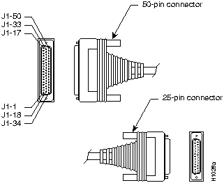
Table A-3 Dual Serial Module EIA/TIA-232 DTE and DCE Serial Cable Pinouts
| 72-0670-01 DTE Connections | 72-0736-01 DCE Connections | ||||||
|---|---|---|---|---|---|---|---|
| 50 Pin | 25 Pin | Type | 50 Pin | 25 Pin | Signal | Type | |
| J1-3 | J1-36 | J1-3 | J1-36 | MUX | |||
| J1-39J1-40 | J2-5J2-4 | Twisted pair | J1-47J1-17 | J2-24J1-38 | SCTEDCE | Twisted pair | |
| J1-9J1-42 | J2-8J2-6 | Twisted pair | J1-40J1-39 | J2-5J2-4 | CTSRTS | Twisted pair | |
| J1-11J1-44 | J2-2J2-7 | Twisted pair | J1-14J1-30 | J2-8J2-6 | DCDDSR | Twisted pair | |
| J1-46J1-30 | J2-3J2-20 | Twisted pair | J1-46J1-44 | J2-2J2-7 | TXDGND | Twisted pair | |
| J1-14J1-47 | J2-18J2-17 | Twisted pair | J1-11J1-42 | J2-3J2-20 | RXDDTR | Twisted pair | |
| J1-31J1-15 | J2-15J2-1 | Twisted pair | J1-9J1-23 | J2-18J2-17 | LTSTRXC | Twisted pair | |
| J1-16 | J2-24 | Twisted pair | J1-16J1-15 | J2-15J2-1 | TXCChassis Ground | Twisted pair | |
Figure A-2 shows the four-port serial module EIA/TIA-232 cable assembly; Table A-4 lists the DTE pinout; and Table A-5 lists the DCE pinout. Arrows indicate signal direction: ---> indicates DTE to DCE, and <--- indicates DCE to DTE.
Figure A-2 EIA/TIA-232 Cable Assembly
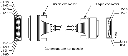
Table A-4 Four-Port Serial EIA/TIA-232 DTE Cable Pinout (DB-60 to DB-25)
| 60 Pin | Signal | Note | Direction | 25 Pin | Signal |
|---|---|---|---|---|---|
| J1-50J1-51J1-52 | MODE_0GNDMODE_DCE | Shorting group | -- | -- | -- |
| J1-46 | Shield GND | Single | -- | J2-1 | Shield GND |
| J1-46 | Shield GND | Single | -- | J2-1 | Shield GND |
| J1-41Shield | TxD/RxD-- | Twisted pair no. 5 | --->-- | J2-2Shield | TxD-- |
| J1-36Shield | RxD/TxD-- | Twisted pair no. 9 | <----- | J2-3Shield | RxD-- |
| J1-42Shield | RTS/CTS-- | Twisted pair no. 4 | --->-- | J2-4Shield | RTS-- |
| J1-35Shield | CTS/RTS-- | Twisted pair no. 10 | <----- | J2-5Shield | CTS-- |
| J1-34Shield | DSR/DTR-- | Twisted pair no. 11 | <----- | J2-6Shield | DSR-- |
| J1-45Shield | Circuit GND-- | Twisted pair no. 1 | ---- | J2-7Shield | Circuit GND-- |
| J1-33Shield | DCD/LL-- | Twisted pair no. 12 | <----- | J2-8Shield | DCD-- |
| J1-37Shield | TxC/NIL-- | Twisted pair no. 8 | <----- | J2-15Shield | TxC-- |
| J1-38Shield | RxC/TxCE-- | Twisted pair no. 7 | <----- | J2-17Shield | RxC-- |
| J1-44Shield | LL/DCD-- | Twisted pair no. 2 | --->-- | J2-18Shield | LTST-- |
| J1-43Shield | DTR/DSR-- | Twisted pair no. 3 | --->-- | J2-20Shield | DTR-- |
| J1-39Shield | TxCE/TxC-- | Twisted pair no. 6 | --->-- | J2-24Shield | TxCE-- |
Table A-5 Four-Port Serial EIA/TIA-232 DCE Cable Pinout (DB-60 to DB-25)
| 60 Pin | Signal | Note | Direction | 25 Pin | Signal |
|---|---|---|---|---|---|
| J1-50J1-51 | MODE_0GND | Shorting group | -- |
-- |
-- |
| J1-36Shield | RxD/TxD-- | Twisted pair no. 9 | <----- | J2-2Shield | TxD-- |
| J1-41Shield | TxD/RxD-- | Twisted pair no. 5 | --->-- | J2-3Shield | RxD-- |
| J1-35Shield | CTS/RTS-- | Twisted pair no. 10 | <----- | J2-4Shield | RTS-- |
| J1-42Shield | RTS/CTS-- | Twisted pair no. 4 | --->-- | J2-5Shield | CTS-- |
| J1-43Shield | DTR/DSR-- | Twisted pair no. 3 | --->-- | J2-6Shield | DSR-- |
| J1-45Shield | Circuit GND-- | Twisted pair no. 1 | ---- | J2-7Shield | Circuit GND |
| J1-44Shield | LL/DCD-- | Twisted pair no. 2 | --->-- | J2-8Shield | DCD-- |
| J1-39Shield | TxCE/TxC-- | Twisted pair no. 7 | --->-- | J2-15Shield | TxC-- |
| J1-40Shield | NIL/RxC-- | Twisted pair no. 6 | --->-- | J2-17Shield | RxC-- |
| J1-33Shield | DCD/LL-- | Twisted pair no. 12 | <----- | J2-18Shield | LTST-- |
| J1-34Shield | DSR/DTR-- | Twisted pair no. 11 | <----- | J2-20Shield | DTR-- |
| J1-38Shield | RxC/TxCE-- | Twisted pair no. 8 | <----- | J2-24Shield | TxCE-- |
Figure A-3 shows the dual serial module EIA/TIA-449 cable assembly. Table A-6 lists the DTE and DCE pinouts and signal descriptions.
Figure A-3 Dual Serial Module EIA/TIA-449 Cable Assembly
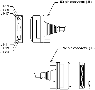
Table A-6 Dual Serial Module EIA/TIA-449 DTE and DCE Cable Pinouts
| 72-0672-01 DTE Connection Table | 72-0738-01 DCE Connection Table | ||||||
|---|---|---|---|---|---|---|---|
| 50 Pin | 37 Pin | Type | 50 Pin | 37 Pin | Type | Signal Name | |
| J1-5 | J1-38 | J1-5 | J1-38 | MUX | |||
| J1-7 | J2-10 | J1-13 | J2-10 | LL | |||
| J1-1J1-34 | J2-4J2-22 | Twisted pair | J1-35J1-19 | J2-4J2-22 | Twisted pair | TXD+TXD- | |
| J1-2J1-18 | J2-5J2-23 | Twisted pair | J1-43J1-27 | J2-5J2-23 | Twisted pair | SCT+SCT- | |
| J1-35J1-19 | J2-6J2-24 | Twisted pair | J1-1J1-34 | J2-6J2-24 | Twisted pair | RXD+RXD- | |
| J1-4J1-20 | J2-7J2-25 | Twisted pair | J1-6J1-22 | J2-7J2-25 | Twisted pair | RTS+RTS- | |
| J1-37J1-21 | J2-8J2-26 | Twisted pair | J1-49J1-50 | J2-8J2-26 | Twisted pair | SCR+SCR- | |
| J1-22J1-6 | J2-27J2-9 | Twisted pair | J1-17 | J1-44 | DCE | ||
| J1-8J1-24 | J2-11J2-29 | Twisted pair | J1-20J1-4 | J2-27J2-9 | Twisted pair | CTS-CTS+ | |
| J1-41J1-25 | J2-12J2-30 | Twisted pair | J1-41J1-25 | J2-11J2-29 | Twisted pair | DSR+DSR- | |
| J1-10J1-26 | J2-13J2-31 | Twisted pair | J1-8J1-24 | J2-12J2-30 | Twisted pair | DTR+DTR- | |
| J1-43J1-27 | J2-17J2-35 | Twisted pair | J1-10J1-26 | J2-13J2-31 | Twisted pair | RLSD+RLSD- | |
| J1-36J1-15 | J2-19J2-1 | Twisted pair | J1-37J1-21 | J2-17J2-35 | Twisted pair | SCTE+SCTE- | |
| J1-44J1-48 | J2-37J2-20 | Twisted pair | J1-36J1-15 | J2-19J2-1 | Twisted pair | GroundChassis Ground | |
Figure A-4 shows the four-port EIA/TIA-449 cable assembly; Table A-7 lists the DTE pinout; Table A-8 lists the DCE pinout. Arrows indicate signal direction: ---> indicates DTE to DCE, and <--- indicates DCE to DTE.
Figure A-4 EIA/TIA-449 Four-Port Module Cable Assembly
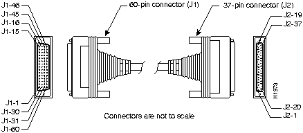
Table A-7 EIA/TIA-449 DTE Cable Pinout (DB-60 to DB-37)
| 60 Pin | Signal Name | Note | Direction | 37 Pin | Signal Name |
|---|---|---|---|---|---|
| J1-49J1-48 | MODE_1GND | Shorting group | -- | -- | -- |
| J1-51J1-52 | GNDMODE_DCE | Shorting group | -- | -- | -- |
| J1-46 | Shield_GND | Single | _ | J2-1 | Shield GND |
| J1-11J1-12 | TxD/RxD+TxD/RxD-- | Twisted pair no. 6 | --->---> | J2-4J2-22 | SD+SD-- |
| J1-24J1-23 | TxC/RxC+TxC/RxC-- | Twisted pair no. 9 | <---<--- | J2-5J2-23 | ST+ST-- |
| J1-28J1-27 | RxD/TxD+RxD/TxD-- | Twisted pair no. 11 | <---<--- | J2-6J2-24 | RD+RD-- |
| J1-9J1-10 | RTS/CTS+RTS/CTS-- | Twisted pair no. 5 | --->---> | J2-7J2-25 | RS+RS-- |
| J1-26J1-25 | RxC/TxCE+RxC/TxCE-- | Twisted pair no. 10 | <---<--- | J2-8J2-26 | RT+RT-- |
| J1-1J1-2 | CTS/RTS+CTS/RTS-- | Twisted pair no. 1 | <---<--- | J2-9J2-27 | CS+CS-- |
| J1-44J1-45 | LL/DCDCircuit_GND | Twisted pair no. 12 | --->_ | J2-10J2-37 | LLSC |
| J1-3J1-4 | DSR/DTR+DSR/DTR-- | Twisted pair no. 2 | <---<--- | J2-11J2-29 | DM+DM-- |
| J1-7J1-8 | DTR/DSR+DTR/DSR-- | Twisted pair no. 4 | --->---> | J2-12J2-30 | TR+TR-- |
| J1-5J1-6 | DCD/DCD+DCD/DCD-- | Twisted pair no. 3 | <---<--- | J2-13J2-31 | RR+RR-- |
| J1-13J1-14 | TxCE/TxC+TxCE/TxC-- | Twisted pair no. 7 | --->---> | J2-17J2-35 | TT+TT-- |
| J1-15J1-16 | Circuit_GNDCircuit_GND | Twisted pair no. 9 | ---- | J2-19J2-20 | SGRC |
Table A-8 EIA/TIA-449 DCE Four-Port Cable Pinout (DB-60 to DB-37)
| 60 Pin | Signal Name | Note | Direction | 37 Pin | Signal Name |
|---|---|---|---|---|---|
| J1-49J1-48 | MODE_1GND | Shorting group | -- | -- | -- |
| J1-46 | Shield_GND | Single | -- | J2-1 | Shield GND |
| J1-28J1-27 | RxD/TxD+RxD/TxD-- | Twisted pair no. 11 | <---<--- | J2-4J2-22 | SD+SD-- |
| J1-13J1-14 | TxCE/TxC+TxCE/TxC-- | Twisted pair no. 7 | --->---> | J2-5J2-23 | ST+ST-- |
| J1-11J1-12 | TxD/RxD+TxD/RxD-- | Twisted pair no. 6 | --->---> | J2-6J2-24 | RD+RD-- |
| J1-1J1-2 | CTS/RTS+CTS/RTS-- | Twisted pair no. 1 | <---<--- | J2-7J2-25 | RS+RS-- |
| J1-24J1-23 | TxC/RxC+TxC/RxC-- | Twisted pair no. 9 | --->---> | J2-8J2-26 | RT+RT-- |
| J1-9J1-10 | RTS/CTS+RTS/CTS-- | Twisted pair no. 5 | --->---> | J2-9J2-27 | CS+CS-- |
| J1-29J1-30 | NIL/LLCircuit_GND | Twisted pair no. 12 | --->-- | J2-10J2-37 | LLSC |
| J1-7J1-8 | DTR/DSR+DTR/DSR-- | Twisted pair no. 4 | --->---> | J2-11J2-29 | DM+DM-- |
| J1-3J1-4 | DSR/DTR+DSR/DTR-- | Twisted pair no. 2 | <---<--- | J2-12J2-30 | TR+TR-- |
| J1-5J1-6 | DCD/DCD+DCD/DCD-- | Twisted pair no. 3 | --->---> | J2-13J2-31 | RR+RR-- |
| J1-26J1-25 | RxC/TxCE+RxC/TxCE-- | Twisted pair no. 10 | <---<--- | J2-17J2-35 | TT+TT-- |
| J1-15J1-16 | Circuit_GNDCircuit_GND | Twisted pair no. 8 | __ | J2-19J2-20 | SGRC |
Figure A-5 shows the dual serial module V.35 cable assembly with the resistor (1/4 watt, ±1%, 301 ohms), and Table A-9 lists the DTE and DCE pinouts.
Figure A-5 Dual Serial Module V.35 Cable Assembly
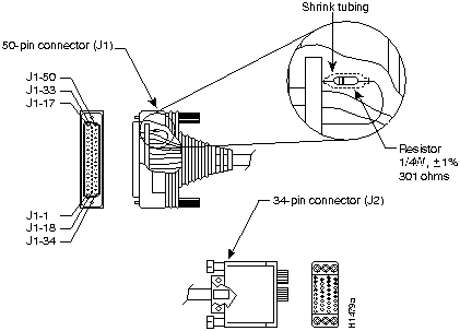
Table A-9 Dual Serial Module V.35 DTE and DCE Cable Pinouts
| 72-0671-02 DTE Connections | 72-0740-02 DCE Connections | |||||||||
|---|---|---|---|---|---|---|---|---|---|---|
| 50 Pin | 34 Pin | Type | Signal Name | Direction | 50 Pin | 34 Pin | Type | Signal Name | Direction | |
| J1-3 | J1-36 | Jumper | MUX | To ground | J1-3 | J1-36 | Jumper | MUX | To ground | |
| J1-5 | J1-38 | Jumper | MUX | To ground | J1-5 | J1-38 | Jumper | MUX | To ground | |
| J1-14J1-Shield | J2-KJ2-Shield | Twisted pair | LTST Not used | ---> | J1-9J1-Shield | J2-KJ2-Shield | Twisted pair | LTST |
<--- | |
| J1-2J1-18 | J2-YJ2-AA | Twisted pair | SCT+SCT- | <---<--- | J1-45J1-29 | J2-YJ2-AA | Twisted pair | SCT+SCT- | --->---> | |
| J1-12J1-28 | J2-PJ2-S | Twisted pair | TXD+TXD- | --->---> | J1-35J1-19 | J2-PJ2-S | Twisted pair | TXD+TXD- | <---<--- | |
| J1-35J1-19 | J2-RJ2-T | Twisted pair | RXD+RXD- | <---<--- | J1-12J1-28 | J2-RJ2-T | Twisted pair | RXD +RXD- | --->---> | |
| J1-37J1-21 | J2-VJ2-X | Twisted pair | SCR+SCR- | <---<--- | J1-32J1-33 | J2-VJ2-X | Twisted pair | SCR+SCR- | --->---> | |
| J1-45J1-29 | J2-UJ2-W | Twisted pair | SCTE+SCTE- | --->---> | J1-37J1-21 | J2-UJ2-W | Twisted pair | SCTE+SCTE- | <---<--- | |
| J1-42J1-Shield | J2-EJ2-Shield | Twisted pair | DSRNot used | <--- | J1-30J1-Shield | J2-EJ2-Shield | Twisted pair | DSR |
---> | |
| J1-9J1-48 | J2-FJ2-A | Twisted pair | RLSDGround | <---<--- | J1-14J1-48 | J2-FJ2-A | Twisted pair | RLSDGround | --->---> | |
| J1-40J1-Shield | J2-CJ2-Shield | Twisted pair | RTSNot used | ---> | J1-39J1-Shield | J2-CJ2-Shield | Twisted pair | RTSNot used | <--- | |
| J1-2J1-18 | J1-3J1-5 | ResistorResistor | SCT+SCT- | R toGround | J1-17 | J1-5 | Jumper | DCE Mode | To ground | |
| J1-35J1-19 | J1-36J1-38 | ResistorResistor | RXD+RXD- | R toGround | J1-Shield | J2-Shield | Single | Not used | ||
| J1-37J1-21 | J1-44J1-48 | ResistorResistor | SCR+SCR- | R toGround | J1-35(1)J1-19 | J1-36J1-38 | ResistorResistor | TXD+TXD- | R to ground | |
| J1-30J1-44 | J2-HJ2-B | Twisted pair | DTRGround | --->---> | J1-37J1-21 | J1-44J1-48 | ResistorResistor | SCTE+SCTE- | R to ground | |
| J1-39J1-Shield | J2-DJ2-Shield | Twisted pair | CTSNot used | ---> | J1-42J1-44 | J2-HJ2-B | Twisted pair | DTRGround | <---<--- | |
| J1-ShieldJ1-Shield | J2-ShieldJ2-Shield | Twisted pair | Not usedNot used | J1-40J1-Shield | J2-DJ2-Shield | Twisted pair | CTSNot used | ---> | ||
| J1-Shield | J2-Shield | Single | Not used | J1-ShieldJ1-Shield | J2-ShieldJ2-Shield | Twisted pair | ||||
Figure A-6 shows the V.35 cable assembly; Table A-10 lists the DTE pinout; Table A-11 lists the DCE pinout. Arrows indicate signal direction: ---> indicates DTE to DCE, and <--- indicates DCE to DTE.
Figure A-6 Four-Port Serial Module V.35 Cable Assembly
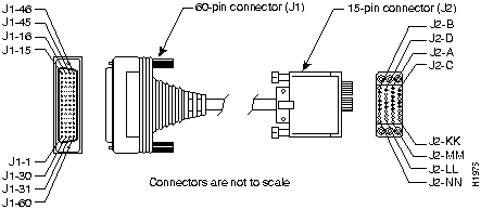
Table A-10 Four-Port Serial Module V.35 DTE Cable Pinout (DB-60 to Winchester-Type 34 Pin)
| 60 Pin | Signal Name | Type | Direction | 34 Pin | Signal Name |
|---|---|---|---|---|---|
| J1-49J1-48 | MODE_1GND | Shorting group | -- | -- | -- |
| J1-50J1-51J1-52 | MODE_0GNDMODE_DCE | Shorting group | -- | -- | -- |
| J1-53J1-54J1-55J1-56 | TxC/NILRxC_TxCERxD/TxDGND | Shorting group | -- | -- | -- |
| J1-46 | Shield_GND | Single | -- | J2-A | Frame GND |
| J1-45Shield | Circuit_GND-- | Twisted pair no. 12 | ---- | J2-BShield | Circuit GND-- |
| J1-42Shield | RTS/CTS-- | Twisted pair no. 9 | --->-- | J2-CShield | RTS-- |
| J1-35Shield | CTS/RTS-- | Twisted pair no. 8 | <----- | J2-DShield | CTS-- |
| J1-34Shield | DSR/DTR-- | Twisted pair no. 7 | <----- | J2-EShield | DSR-- |
| J1-33Shield | DCD/LL-- | Twisted pair no. 6 | <----- | J2-FShield | RLSD-- |
| J1-43Shield | DTR/DSR-- | Twisted pair no. 10 | --->-- | J2-HShield | DTR-- |
| J1-44Shield | LL/DCD-- | Twisted pair no. 11 | --->-- | J2-KShield | LT-- |
| J1-18J1-17 | TxD/RxD+TxD/RxD-- | Twisted pair no. 1 | --->---> | J2-PJ2-S | SD+SD-- |
| J1-28J1-27 | RxD/TxD+RxD/TxD-- | Twisted pair no. 5 | <---<--- | J2-RJ2-T | RD+RD-- |
| J1-20J1-19 | TxCE/TxC+TxCE/TxC-- | Twisted pair no. 2 | --->---> | J2-UJ2-W | SCTE+SCTE-- |
| J1-26J1-25 | RxC/TxCE+RxC/TxCE-- | Twisted pair no. 4 | <---<--- | J2-VJ2-X | SCR+SCR-- |
| J1-24J1-23 | TxC/RxC+TxC/RxC-- | Twisted pair no. 3 | <---<--- | J2-YJ2-AA | SCT+SCT-- |
Table A-11 Four-Port Serial V.35 DCE Cable Pinout (DB-60 to Winchester-Type 34 Pin)
| 60 Pin | Signal Name | Type | Direction | 34 Pin | Signal Name |
|---|---|---|---|---|---|
| J1-49J1-48 | MODE_1GND | Shorting group | -- | -- | -- |
| J1-50J1-51 | MODE_0GND | Shorting group | -- | -- | -- |
| J1-53J1-54J1-55J1-56 | TxC/NILRxC_TxCERxD/TxDGND | Shorting group | -- | -- | -- |
| J1-46 | Shield_GND | Single | -- | J2-A | Frame GND |
| J1-45Shield | Circuit_GND-- | Twisted pair no. 12 | ---- | J2-BShield | Circuit GND-- |
| J1-35Shield | CTS/RTS-- | Twisted pair no. 8 | <----- | J2-CShield | RTS-- |
| J1-42Shield | RTS/CTS-- | Twisted pair no. 9 | --->-- | J2-DShield | CTS-- |
| J1-43Shield | DTR/DSR-- | Twisted pair no. 10 | --->-- | J2-EShield | DSR-- |
| J1-44Shield | LL/DCD-- | Twisted pair no. 11 | --->-- | J2-FShield | RLSD-- |
| J1-34Shield | DSR/DTR-- | Twisted pair no. 7 | <----- | J2-HShield | DTR-- |
| J1-33Shield | DCD/LL-- | Twisted pair no. 6 | <----- | J2-KShield | LT-- |
| J1-28J1-27 | RxD/TxD+RxD/TxD-- | Twisted pair no. 5 | <---<--- | J2-PJ2-S | SD+SD-- |
| J1-18J1-17 | TxD/RxD+TxD/RxD-- | Twisted pair no. 1 | --->---> | J2-RJ2-T | RD+RD-- |
| J1-26J1-25 | RxC/TxCE+RxC/TxCE-- | Twisted pair no. 4 | <---<--- | J2-UJ2-W | SCTE+SCTE-- |
| J1-22J1-21 | NIL/RxC+NIL/RxC-- | Twisted pair no. 3 | --->---> | J2-VJ2-X | SCR+SCR-- |
| J1-20J1-19 | TxCE/TxC+TxCE/TxC-- | Twisted pair no. 2 | --->---> | J2-YJ2-AA | SCT+SCT-- |
Figure A-7 shows the dual serial module X.21 cable assembly. Table A-12 lists DTE and DCE pinouts.
Figure A-7 Dual Serial Module X.21 Cable Assembly
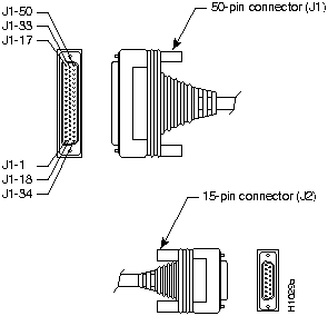
Table A-12 Dual Serial Module X.21 DTE and DCE Cable Pinouts
| 72-0683-02 DTE Connections | 72-0737-01 DCE Connections | ||||||||
|---|---|---|---|---|---|---|---|---|---|
| From | Signal Name | Type | To | Signal Name | From | Signal Name | Type | To | Signal Name |
| J1-5 | MUX SEL | J1-38 | GND | J1-5 | MUX SEL | J1-38 | GND | ||
| J1-36 | 449 GND | J2-8 | X.21 GND | J1-36 | 449 GND | J2-8 | X.21 GND | ||
| J1-41J1-25 | 449 DTR | Jumper | J1-6J1-22 | 449 CTS | J1-41J1-25 | 449 DSR | Jumper | J1-8J1-24 | 449 DTR |
| J1-41J1-25 | 449 DTR | Jumper | J1-8J1-24 | 449 DSR | J1-35J1-19 | 449 TXD | Twisted pair | J2-2J2-9 | X.21 TXD |
| J1-43J1-27 | 449 SCTE | Jumper | J1-37J1-21 | 449 SCR | J1-6J1-22 | 449-RTS | Twisted pair | J2-3J2-10 | X.21 CTL |
| J1-1J1-34 | 449 TXD | Twisted pair | J2-2J2-9 | X.21 TXD | J1-1J1-34 | 449 RXD | Twisted pair | J2-4J2-11 | X.21 RXD |
| J1-4J1-20 | 449 RTS | Twisted pair | J2-3J2-10 | X.21 CTL | J1-10J1-26 | 449 RLSD | Twisted pair | J2-5J2-12 | X.21 IND |
| J1-35J1-19 | 449 RXD | Twisted pair | J2-4J2-11 | X.21 RXD | J1-43J1-27 | 449 SCT | Twisted pair | J2-6J2-13 | X.21 CLK |
| J1-10J1-26 | 449 RLSD | Twisted pair | J2-5J2-12 | X.21 IND | J1-17 | DCE SEL | J1-44 | ||
| J1-2J1-18 | 449 SCT | Twisted pair | J2-6J2-13 | X.21 CLK | J1-15 | Chassis GND | J2-1 | ||
Figure A-8 shows the four-port serial X.21 cable assembly; Table A-13 lists the DTE pinout; Table A-14 lists the DCE pinout. Arrows indicate signal direction: ---> indicates DTE to DCE, and <--- indicates DCE to DTE.
Figure A-8 Four-Port Serial Module X.21 Cable Assembly
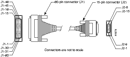
Table A-13 Four-Port Serial X.21 DTE Cable Pinout (DB-60 to DB-15)
| 60 Pin | Signal Name | Type | Direction | 15 Pin | Signal Name |
|---|---|---|---|---|---|
| J1-48J1-47 | GNDMODE_2 | Shorting group | - | -- | -- |
| J1-51J1-52 | GNDMODE_DCE | Shorting group | -- | -- | -- |
| J1-46 | Shield_GND | Single | -- | J2-1 | Shield GND |
| J1-11J1-12 | TxD/RxD+TxD/RxD-- | Twisted pair no. 3 | --->---> | J2-2J2-9 | Transmit+Transmit-- |
| J1-9J1-10 | RTS/CTS+RTS/CTS-- | Twisted pair no. 2 | --->---> | J2-3J2-10 | Control+Control-- |
| J1-28J1-27 | RxD/TxD+RxD/TxD-- | Twisted pair no. 6 | <---<--- | J2-4J2-11 | Receive+Receive-- |
| J1-1J1-2 | CTS/RTS+CTS/RTS-- | Twisted pair no. 1 | <---<--- | J2-5J2-12 | Indication+Indication-- |
| J1-26J1-25 | RxC/TxCE+RxC/TxCE-- | Twisted pair no. 5 | <---<--- | J2-6J2-13 | Timing+Timing-- |
| J1-15Shield | Control_GND-- | Twisted pair no. 4 | ---- | J2-8Shield | Control GND-- |
Table A-14 Four-Port Serial X.21 DCE Cable Pinout (DB-60 to DB-15)
| 60 Pin | Signal Name | Type | Direction | 15 Pin | Signal Name |
|---|---|---|---|---|---|
| J1-48J1-47 | GNDMODE_2 | Shorting group | -- | -- | -- |
| J1-46 | Shield_GND | Single | -- | J2-1 | Shield GND |
| J1-28J1-27 | RxD/TxD+RxD/TxD-- | Twisted pair no. 6 | <---<--- | J2-2J2-9 | Transmit+Transmit-- |
| J1-1J1-2 | CTS/RTS+CTS/RTS-- | Twisted pair no. 1 | <---<--- | J2-3J2-10 | Control+Control-- |
| J1-11J1-12 | TxD/RxD+TxD/RxD-- | Twisted pair no. 3 | --->---> | J2-4J2-11 | Receive+Receive-- |
| J1-9J1-10 | RTS/CTS+RTS/CTS-- | Twisted pair no. 2 | --->---> | J2-5J2-12 | Indication+Indication-- |
| J1-24J1-23 | TxC/RxC+TxC/RxC-- | Twisted pair no. 4 | --->---> | J2-6J2-13 | Timing+Timing-- |
| J1-15Shield | Control_GND-- | Twisted pair no. 5 | ---- | J2-8Shield | Control GND-- |
Figure A-9 shows the dual serial module EIA-530 cable assembly and Table A-15 lists the EIA-530 DTE serial cable pinout.
Figure A-9 Dual Serial Module EIA-530 Cable Assembly

Table A-15 Dual Serial Module EIA-530 DTE Serial Cable Pinout
| 72-0732-01 Connections | ||||
|---|---|---|---|---|
| 50 Pin | Signal Name | Direction | 25 Pin | Type |
| J1-5J1-38 | Looped | NC | Jumper | |
| J1-1J1-34 | TXD +TXD - | --->---> | J2-2J2-14 | Twisted pair |
| J1-35J1-19 | RXD +RXD - | <---<--- | J2-3J2-16 | Twisted pair |
| J1-4J1-20 | RTS +RTS - | --->---> | J2-4J2-19 | Twisted pair |
| J1-6J1-22 | CTS + CTS - | <---<--- | J2-5J2-13 | Twisted pair |
| J1-10J1-26 | RLSD + (RR+) RLSD - (RR-) | <---<--- | J2-8J2-10 | Twisted pair |
| J1-2J1-18 | SCT + SCT - | <---<--- | J2-15J2-12 | Twisted pair |
| J1-37J1-21 | SCR +SCR - | <---<--- | J2-17J2-9 | Twisted pair |
| J1-43J1-27 | SCTE + (TT+)SCTE - (TT-) | <---<--- | J2-24J2-11 | Twisted pair |
| J1-7 | LL | ---> | J2-18 | Twisted pair |
| J1-48J1-36 | Ground | J2-23J2-7 | Twisted pair | |
| J1-15 | Shield | J2-1 | Single Wire | |
| J1-8J1-24 | DCE Ready Ground | <--- | J2-6J2-23 | Twisted pair |
| J1-41 | DTE Ready | ---> | J2-20 | Twisted pair |
Figure A-10 shows the four-port serial module EIA-530 cable assembly, and Table A-16 lists the pinouts. Arrows indicate signal direction: ---> indicates DTE to DCE, and <--- indicates DCE to DTE.
Figure A-10 Four-Port Serial Module EIA-530 Cable Assembly
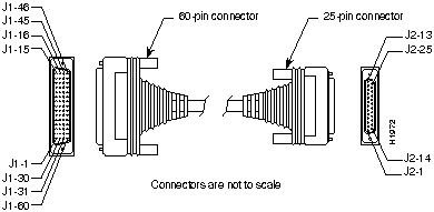
Table A-16 Four-Port Serial EIA-530 DTE Cable Pinout (DB-60 to DB-25)
| 60 Pin | Signal Name | 25 Pin | Signal Name | DirectionDTE DCE(1) | 60 Pin | Signal Name | 25 Pin | Signal Name | DirectionDTE DCE1 |
|---|---|---|---|---|---|---|---|---|---|
| J1-11J1-12 | TxD/RxD+TxD/RxD-- | J2-2J2-14 | BA(A), TxD+BA(B), TxD-- | --->---> | J1-5J1-6 | DCD/DCD+DCD/DCD-- | J2-8J2-10 | CF(A), DCD+CF(B), DCD-- | <---<--- |
| J1-28J1-27 | RxD/TxD+RxD/TxD-- | J2-3J2-16 | BB(A), RxD+BB(B), RxD-- | <---<--- | J1-24J1-23 | TxC/RxC+TxC/RxC-- | J2-15J2-12 | DB(A), TxC+DB(B), TxC-- | <---<--- |
| J1-9J1-10 | RTS/CTS+RTS/CTS-- | J2-4J2-19 | CA(A), RTS+CA(B), RTS-- | --->---> | J1-26J1-25 | RxC/TxCE+RxC/TxCE-- | J2-17J2-9 | DD(A), RxC+DD(B), RxC-- | <---<--- |
| J1-1J1-2 | CTS/RTS+CTS/RTS-- | J2-5J2-13 | CB(A), CTS+ CB(B), CTS-- | <---<--- | J1-44J1-45 | LL/DCDCircuit_GND | J2-18J2-7 | LL Circuit_ GND | --->-- |
| J1-3J1-4 | DSR/DTR+DSR/DTR-- | J2-6J2-22 | CC(A), DSR+ CC(B), DSR-- | <---<--- | J1-7J1-8 | DTR/DSR+DTR/DSR-- | J2-20J2-23 | CD(A), DTR+CD(B), DTR-- | --->---> |
| J1-46J1-47 | Shield_GNDMODE_2 | J2-1-- | Shield-- | Shorted | J1-13J1-14 | TxCE/TxC+TxCE/TxC-- | J2-24J2-11 | DA(A), TxCE+DA(B), TxCE-- | --->---> |
| J1-48J1-49 | GNDMODE_1 | ---- | ---- | Shorted | J1-51J1-52 | GNDMODE_DCE | ---- | ---- | Shorted |
The following figures and tables provide the pinouts and signal descriptions for the Ethernet (AUI) cable and RJ-45 connector.
Figure A-11 shows the Ethernet (AUI) cable assembly, and Table A-17 lists the pinout.
Figure A-11 Ethernet (AUI) Cable Assembly
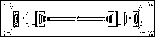
Table A-17 Ethernet (AUI) Pinout
| Pin(1) | Ethernet Circuit | Signal Name |
|---|---|---|
| 3 | DO-A | Data Out Circuit A |
| 10 | DO-B | Data Out Circuit B |
| 11 | DO-S | Data Out Circuit Shield |
| 5 | DI-A | Data In Circuit A |
| 12 | DI-B | Data In Circuit B |
| 4 | DI-S | Data In Circuit Shield |
| 7 | CO-A | Control Out Circuit A (not connected) |
| 15 | CO-B | Control Out Circuit B (not connected) |
| 8 | CO-S | Control Out Circuit Shield (not connected) |
| 2 | CI-A | Control In Circuit A |
| 9 | CI-B | Control In Circuit B |
| 1 | CI-S | Control In Circuit Shield |
| 6 | VC | Voltage Common |
| 13 | VP | Voltage Plus |
| 14 | VS | Voltage Shield (L25 and M25) |
| Shell | PG | Protective Ground |
Figure A-12 shows the RJ-45 10BaseT connector, and Table A-18 lists the pinout.
Figure A-12 RJ-45 10BaseT Connector
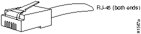
Table A-18 RJ-45 Connector Pinout
| Pin(1) | Description |
|---|---|
| 1 | TX+ |
| 2 | TX- |
| 3 | RX+ |
| 4 | -- |
| 5 | -- |
| 6 | RX- |
| 7 | -- |
| 8 | -- |
Table A-19 shows the original single-port Token Ring network processor module (Cisco product number NP-1R) port pinout:
Table A-19 Token Ring Port Pinout (DB-9 Connector)
| 9-Pin | Signal Name |
|---|---|
| 1 | --RX |
| 2 | NC(1) |
| 3 | NC |
| 4 | NC |
| 5 | --TX |
| 6 | +RX |
| 7 | NC |
| 8 | NC |
| 9 | +TX |
Table A-20 shows the dual-port and newer single-port (Cisco product numbers NP-2R and NP-1RV2) Token Ring network processor module port pinout:
Table A-20 Dual-Port Token Ring Pinout (DB-9 Connector)
| 9-Pin | Signal Name |
|---|---|
| 1 | --RX |
| 2 | Ground |
| 3 | +5 Volt, fused |
| 4 | Ground |
| 5 | --TX |
| 6 | +RX |
| 7 | Ground |
| 8 | Ground |
| 9 | +TX |
The BRI interface port pinout is shown in Table A-21.
Table A-21 BRI Port Pinout (RJ-45)
| 8 Pin(1) | TE(2) | NT(3) | Polarity |
|---|---|---|---|
| 3 | Transmit | Receive | + |
| 4 | Receive | Transmit | + |
| 5 | Receive | Transmit | -- |
| 6 | Transmit | Receive | -- |
![]()
For the CT1, two standard T1 serial cables are available from Cisco Systems: null-modem and straight-through. A straight through cable connect your router to an external CSU. Null modem cables are used for back-to-back operation and testing.
The cables have male 15-pin DB connectors at each end to connect the CT1with the external CSU.
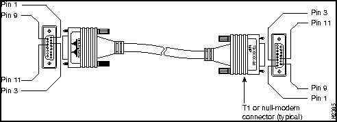
The T1 interface cable has two 15-pin DB connectors at each end to connect the CT1with the external T1 CSU. Figure A-13 shows the T1 interface cable, connectors and pin-outs.
Figure A-13 T1 Interface Cable
The T1 interface cables have two, male, 15-pin DB connectors (one at each end) to connect the CT1 with the external CSU. Table A-22 lists the pinouts for the null-modem T1 cable and Table A-23 lists the pinouts for the straight-through T1 cable.
Table A-22 T1 Null-Modem Cable Pinouts (P/N 72-0800-xx)
| 15-Pin DB Connector | 15-Pin DB Connector | ||
|---|---|---|---|
| Signal | Pin | Pin | Signal |
| Transmit tip | 1 | 3 | Receive tip |
| Receive tip | 3 | 1 | Transmit tip |
| Transmit ring | 9 | 11 | Receive ring |
| Receive ring | 11 | 9 | Transmit ring |
Table A-23 T1 Straight-Through Cable Pinouts (P/N 72-0799-xx)
| 15-Pin DB Connector | 15-Pin DB Connector | ||
|---|---|---|---|
| Signal | Pin | Pin | Signal |
| Transmit tip | 1 | 1 | Transmit tip |
| Transmit ring | 9 | 9 | Transmit ring |
| Receive tip | 3 | 3 | Receive tip |
| Receive ring | 11 | 11 | Receive ring |
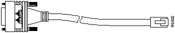
For the CE1 module, four serial cables are available from Cisco Systems. All three have DB-15 connectors on the CE1end and either BNC, DB-15, Twinax, or RJ-45 connectors on the network end. Figure A-14, Figure A-15, Figure A-16, and Figure A-17 show the E1 interface cables (respectively).
Figure A-14 E1 Interface Cable for 75-Ohm, Unbalanced Connections (with BNC Connectors)
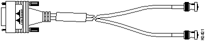
Figure A-15 E1 Interface Cable for 120-Ohm, Balanced Connections (with DB-15 Connectors)
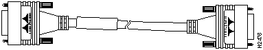
Figure A-16 E1 Interface Cable for 120-Ohm, Balanced Connections (with Twinax Connectors)
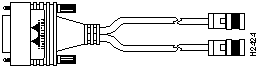
Figure A-17 E1 Interface Cable for 120-Ohm, Balanced Connections (with RJ-45 Connector)
The E1 interface cables have two, male, 15-pin DB connectors (one at each end) to connect the CE1with the external CSU. Table A-24 lists the pinouts for the E1 interface cables available from Cisco Systems.
Table A-24 E1 Interface Cable Pinouts
| CE1 End | Network End | |||||||
|---|---|---|---|---|---|---|---|---|
| DB-15(1) | BNC | DB-15 | Twinax | RJ-45 | ||||
| Pin | Signal(2) | Signal | Pin | Signal | Pin | Signal | Pin | Signal |
| 9 | Tx tip | Tx tip | 1 | Tx tip | Tx-1 | Tx tip | 1 | Tx tip |
| 2 | Tx ring | Tx shield | 9 | Tx ring | Tx-2 | Tx ring | 2 | Tx ring |
| 10 | Tx shield | -- | 2 | Tx shield | Shield | Tx shield | 3 | Tx shield |
| 8 | Rx tip | Rx tip | 3 | Rx tip | Rx-1 | Rx tip | 4 | Rx tip |
| 15 | Rx ring | Rx shield | 11 | Rx ring | Rx-2 | Rx ring | 5 | Rx ring |
| 7 | Rx shield | -- | 4 | Rx shield | Shield | Rx shield | 6 | Rx shield |
|
|
Copyright 1988-1995 © Cisco Systems Inc.