The following illustrations and tables provide assembly drawings and pinouts for the EIA-530 DCE, and EIA/TIA-232, EIA/TIA-449, V.35, and X.21 DTE and DCE cables.
Note All serial cables have a DB-60 connector on the router end. The following pinouts represent only the router ends of the cables. Because of the small pins on the DB-60 connector, manufacturing and soldering these cables yourself might be very difficult and is not recommended.
EIA-530
Figure A-1 shows the EIA-530 serial cable assembly, and Table A-4 lists the pinouts. Arrows indicate signal direction. A right arrow (--->) indicates DTE to DCE, and a left arrow (<---) indicates DCE to DTE.
Figure A-1 : EIA-530 Serial Cable Assembly
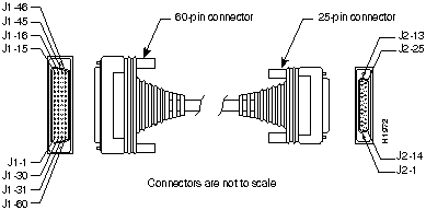
Table A-4 : EIA-530 DTE Cable Pinouts (DB-60 to DB-25)
J1-11
J1-12
|
TxD/RxD+
TxD/RxD--
|
J2-2
J2-14
|
BA(A), TxD+
BA(B), TxD--
|
--->
--->
|
J1-5
J1-6
|
DCD/DCD+
DCD/DCD--
|
J2-8
J2-10
|
CF(A), DCD+
CF(B), DCD--
|
<---
<---
|
J1-28
J1-27
|
RxD/TxD+
RxD/TxD--
|
J2-3
J2-16
|
BB(A), RxD+
BB(B), RxD--
|
<---
<---
|
J1-24
J1-23
|
TxC/RxC+
TxC/RxC--
|
J2-15
J2-12
|
DB(A), TxC+
DB(B), TxC--
|
<---
<---
|
J1-9
J1-10
|
RTS/CTS+
RTS/CTS--
|
J2-4
J2-19
|
CA(A), RTS+
CA(B), RTS--
|
--->
--->
|
J1-26
J1-25
|
RxC/TxCE+
RxC/TxCE--
|
J2-17
J2-9
|
DD(A), RxC+
DD(B), RxC--
|
<---
<---
|
J1-1
J1-2
|
CTS/RTS+
CTS/RTS--
|
J2-5
J2-13
|
CB(A), CTS+
CB(B), CTS--
|
<---
<---
|
J1-44
J1-45
|
LL/DCD
Circuit_GND
|
J2-18
J2-7
|
LL
Circuit_ GND
|
--->
--
|
J1-3
J1-4
|
DSR/DTR+
DSR/DTR--
|
J2-6
J2-22
|
CC(A), DSR+
CC(B), DSR--
|
<---
<---
|
J1-7
J1-8
|
DTR/DSR+
DTR/DSR--
|
J2-20
J2-23
|
CD(A), DTR+
CD(B), DTR--
|
--->
--->
|
J1-46
J1-47
|
Shield_GND
MODE_2
|
J2-1
--
|
Shield
--
|
Shorted
|
J1-13
J1-14
|
TxCE/TxC+
TxCE/TxC--
|
J2-24
J2-11
|
DA(A), TxCE+
DA(B), TxCE--
|
--->
--->
|
J1-48
J1-49
|
GND
MODE_1
|
--
--
|
--
--
|
Shorted
|
J1-51
J1-52
|
GND
MODE_DCE
|
--
--
|
--
--
|
Shorted
|
1 Any pin not referenced is not connected.
2 The EIA-530 interface cannot be operated in DCE mode. A DCE cable is not available for the EIA-530 interface.
EIA/TIA-232
Figure A-2 shows the EIA/TIA-232 cable assembly; Table A-5 lists the DTE pinouts; and Table A-6 lists the DCE pinouts. Arrows indicate signal direction. A right arrow (--->) indicates DTE to DCE, and a left arrow (<---) indicates DCE to DTE.
Figure A-2 : EIA/TIA-232 Cable Assembly
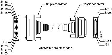
Table A-5 : EIA/TIA-232 DTE Cable Pinouts (DB-60 to DB-25)
J1-50
J1-51
J1-52
|
MODE_0
GND
MODE_DCE
|
Shorting Group
|
--
|
--
|
--
|
| J1-46
|
Shield GND
|
Single
|
--
|
J2-1
|
Shield GND
|
J1-41
Shield
|
TxD/RxD
--
|
Twisted pair no. 5
|
--->
--
|
J2-2
Shield
|
TxD
--
|
J1-36
Shield
|
RxD/TxD
--
|
Twisted pair no. 9
|
<---
--
|
J2-3
Shield
|
RxD
--
|
J1-42
Shield
|
RTS/CTS
--
|
Twisted pair no. 4
|
--->
--
|
J2-4
Shield
|
RTS
--
|
J1-35
Shield
|
CTS/RTS
--
|
Twisted pair no. 10
|
<---
--
|
J2-5
Shield
|
CTS
--
|
J1-34
Shield
|
DSR/DTR
--
|
Twisted pair no. 11
|
<---
--
|
J2-6
Shield
|
DSR
--
|
J1-45
Shield
|
Circuit GND
--
|
Twisted pair no. 1
|
--
--
|
J2-7
Shield
|
Circuit GND
--
|
J1-33
Shield
|
DCD/LL
--
|
Twisted pair no. 12
|
<---
--
|
J2-8
Shield
|
DCD
--
|
J1-37
Shield
|
TxC/NIL
--
|
Twisted pair no. 8
|
<---
--
|
J2-15
Shield
|
TxC
--
|
J1-38
Shield
|
RxC/TxCE
--
|
Twisted pair no. 7
|
<---
--
|
J2-17
Shield
|
RxC
--
|
J1-44
Shield
|
LL/DCD
--
|
Twisted pair no. 2
|
--->
--
|
J2-18
Shield
|
LTST
--
|
J1-43
Shield
|
DTR/DSR
--
|
Twisted pair no. 3
|
--->
--
|
J2-20
Shield
|
DTR
--
|
J1-39
Shield
|
TxCE/TxC
--
|
Twisted pair no. 6
|
--->
--
|
J2-24
Shield
|
TxCE
--
|
1 Any pin not referenced is not connected.
Table A-6 : EIA/TIA-232 DCE Cable Pinouts (DB-60 to DB-25)
J1-50
J1-51
|
MODE_0
GND
|
Shorting Group
|
--
|
--
|
--
|
| J1-46
|
Shield GND
|
Single
|
--
|
J2-1
|
Shield GND
|
J1-36
Shield
|
RxD/TxD
--
|
Twisted pair no. 9
|
<---
--
|
J2-2
Shield
|
TxD
--
|
J1-41
Shield
|
TxD/RxD
--
|
Twisted pair no. 5
|
--->
--
|
J2-3
Shield
|
RxD
--
|
J1-35
Shield
|
CTS/RTS
--
|
Twisted pair no. 10
|
<---
--
|
J2-4
Shield
|
RTS
--
|
J1-42
Shield
|
RTS/CTS
--
|
Twisted pair no. 4
|
--->
--
|
J2-5
Shield
|
CTS
--
|
J1-43
Shield
|
DTR/DSR
--
|
Twisted pair no. 3
|
--->
--
|
J2-6
Shield
|
DSR
--
|
J1-45
Shield
|
Circuit GND
--
|
Twisted pair no. 1
|
--
--
|
J2-7
Shield
|
Circuit GND
|
J1-44
Shield
|
LL/DCD
--
|
Twisted pair no. 2
|
--->
--
|
J2-8
Shield
|
DCD
--
|
J1-39
Shield
|
TxCE/TxC
--
|
Twisted pair no. 7
|
--->
--
|
J2-15
Shield
|
TxC
--
|
J1-40
Shield
|
NIL/RxC
--
|
Twisted pair no. 6
|
--->
--
|
J2-17
Shield
|
RxC
--
|
J1-33
Shield
|
DCD/LL
--
|
Twisted pair no. 12
|
<---
--
|
J2-18
Shield
|
LTST
--
|
J1-34
Shield
|
DSR/DTR
--
|
Twisted pair no. 11
|
<---
--
|
J2-20
Shield
|
DTR
--
|
J1-38
Shield
|
RxC/TxCE
--
|
Twisted pair no. 8
|
<---
--
|
J2-24
Shield
|
TxCE
--
|
1 Any pin not referenced is not connected.
EIA/TIA-449
Figure A-3 shows the EIA/TIA-449 cable assembly; Table A-7 lists the DTE pinouts; Table A-8 lists the DCE pinouts. Arrows indicate signal direction. A right arrow (--->) indicates DTE to DCE, and a left arrow (<---) indicates DCE to DTE.
Figure A-3 : EIA/TIA-449 Cable Assembly
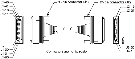
Table A-7 : EIA/TIA-449 DTE Cable Pinouts (DB-60 to DB-37)
J1-49
J1-48
|
MODE_1
GND
|
Shorting Group
|
--
|
--
|
--
|
J1-51
J1-52
|
GND
MODE_DCE
|
Shorting Group
|
--
|
--
|
--
|
| J1-46
|
Shield_GND
|
Single
|
_
|
J2-1
|
Shield GND
|
J1-11
J1-12
|
TxD/RxD+
TxD/RxD--
|
Twisted pair no. 6
|
--->
--->
|
J2-4
J2-22
|
SD+
SD--
|
J1-24
J1-23
|
TxC/RxC+
TxC/RxC--
|
Twisted pair no. 9
|
<---
<---
|
J2-5
J2-23
|
ST+
ST--
|
J1-28
J1-27
|
RxD/TxD+
RxD/TxD--
|
Twisted pair no. 11
|
<---
<---
|
J2-6
J2-24
|
RD+
RD--
|
J1-9
J1-10
|
RTS/CTS+
RTS/CTS--
|
Twisted pair no. 5
|
--->
--->
|
J2-7
J2-25
|
RS+
RS--
|
J1-26
J1-25
|
RxC/TxCE+
RxC/TxCE--
|
Twisted pair no. 10
|
<---
<---
|
J2-8
J2-26
|
RT+
RT--
|
J1-1
J1-2
|
CTS/RTS+
CTS/RTS--
|
Twisted pair no. 1
|
<---
<---
|
J2-9
J2-27
|
CS+
CS--
|
J1-44
J1-45
|
LL/DCD
Circuit_GND
|
Twisted pair no. 12
|
--->
_
|
J2-10
J2-37
|
LL
SC
|
J1-3
J1-4
|
DSR/DTR+
DSR/DTR--
|
Twisted pair no. 2
|
<---
<---
|
J2-11
J2-29
|
DM+
DM--
|
J1-7
J1-8
|
DTR/DSR+
DTR/DSR--
|
Twisted pair no. 4
|
--->
--->
|
J2-12
J2-30
|
TR+
TR--
|
J1-5
J1-6
|
DCD/DCD+
DCD/DCD--
|
Twisted pair no. 3
|
<---
<---
|
J2-13
J2-31
|
RR+
RR--
|
J1-13
J1-14
|
TxCE/TxC+
TxCE/TxC--
|
Twisted pair no. 7
|
--->
--->
|
J2-17
J2-35
|
TT+
TT--
|
J1-15
J1-16
|
Circuit_GND
Circuit_GND
|
Twisted pair no. 9
|
--
--
|
J2-19
J2-20
|
SG
RC
|
1 Any pin not referenced is not connected.
Table A-8 : EIA/TIA-449 DCE Cable Pinouts (DB-60 to DB-37)
J1-49
J1-48
|
MODE_1
GND
|
Shorting group
|
--
|
--
|
--
|
| J1-46
|
Shield_GND
|
Single
|
--
|
J2-1
|
Shield GND
|
J1-28
J1-27
|
RxD/TxD+
RxD/TxD--
|
Twisted pair no. 11
|
<---
<---
|
J2-4
J2-22
|
SD+
SD--
|
J1-13
J1-14
|
TxCE/TxC+
TxCE/TxC--
|
Twisted pair no. 7
|
--->
--->
|
J2-5
J2-23
|
ST+
ST--
|
J1-11
J1-12
|
TxD/RxD+
TxD/RxD--
|
Twisted pair no. 6
|
--->
--->
|
J2-6
J2-24
|
RD+
RD--
|
J1-1
J1-2
|
CTS/RTS+
CTS/RTS--
|
Twisted pair no. 1
|
<---
<---
|
J2-7
J2-25
|
RS+
RS--
|
J1-24
J1-23
|
TxC/RxC+
TxC/RxC--
|
Twisted pair no. 9
|
--->
--->
|
J2-8
J2-26
|
RT+
RT--
|
J1-9
J1-10
|
RTS/CTS+
RTS/CTS--
|
Twisted pair no. 5
|
--->
--->
|
J2-9
J2-27
|
CS+
CS--
|
J1-29
J1-30
|
NIL/LL
Circuit_GND
|
Twisted pair no. 12
|
--->
--
|
J2-10
J2-37
|
LL
SC
|
J1-7
J1-8
|
DTR/DSR+
DTR/DSR--
|
Twisted pair no. 4
|
--->
--->
|
J2-11
J2-29
|
DM+
DM--
|
J1-3
J1-4
|
DSR/DTR+
DSR/DTR--
|
Twisted pair no. 2
|
<---
<---
|
J2-12
J2-30
|
TR+
TR--
|
J1-5
J1-6
|
DCD/DCD+
DCD/DCD--
|
Twisted pair no. 3
|
--->
--->
|
J2-13
J2-31
|
RR+
RR--
|
J1-26
J1-25
|
RxC/TxCE+
RxC/TxCE--
|
Twisted pair no. 10
|
<---
<---
|
J2-17
J2-35
|
TT+
TT--
|
J1-15
J1-16
|
Circuit_GND
Circuit_GND
|
Twisted pair no. 8
|
_
_
|
J2-19
J2-20
|
SG
RC
|
1 Any pin not referenced is not connected.
V.35
Figure A-4 shows the V.35 cable assembly; Table A-9 lists the DTE pinouts; Table A-10 lists the DCE pinouts. Arrows indicate signal direction. A right arrow (--->) indicates DTE to DCE, and a left arrow (<---) indicates DCE to DTE.
Figure A-4 : V.35 Cable Assembly
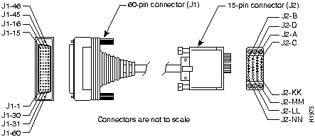
Table A-9 : V.35 DTE Cable Pinouts (DB-60 to 34-Pin)
J1-49
J1-48
|
MODE_1
GND
|
Shorting Group
|
--
|
--
|
--
|
J1-50
J1-51
J1-52
|
MODE_0
GND
MODE_DCE
|
Shorting Group
|
--
|
--
|
--
|
J1-53
J1-54
J1-55
J1-56
|
TxC/NIL
RxC_TxCE
RxD/TxD
GND
|
Shorting Group
|
--
|
--
|
--
|
| J1-46
|
Shield_GND
|
Single
|
--
|
J2-A
|
Frame GND
|
J1-45
Shield
|
Circuit_GND
--
|
Twisted pair no. 12
|
--
--
|
J2-B
Shield
|
Circuit GND
--
|
J1-42
Shield
|
RTS/CTS
--
|
Twisted pair no. 9
|
--->
--
|
J2-C
Shield
|
RTS
--
|
J1-35
Shield
|
CTS/RTS
--
|
Twisted pair no. 8
|
<---
--
|
J2-D
Shield
|
CTS
--
|
J1-34
Shield
|
DSR/DTR
--
|
Twisted pair no. 7
|
<---
--
|
J2-E
Shield
|
DSR
--
|
J1-33
Shield
|
DCD/LL
--
|
Twisted pair no. 6
|
<---
--
|
J2-F
Shield
|
RLSD
--
|
J1-43
Shield
|
DTR/DSR
--
|
Twisted pair no. 10
|
--->
--
|
J2-H
Shield
|
DTR
--
|
J1-44
Shield
|
LL/DCD
--
|
Twisted pair no. 11
|
--->
--
|
J2-K
Shield
|
LT
--
|
J1-18
J1-17
|
TxD/RxD+
TxD/RxD--
|
Twisted pair no. 1
|
--->
--->
|
J2-P
J2-S
|
SD+
SD--
|
J1-28
J1-27
|
RxD/TxD+
RxD/TxD--
|
Twisted pair no. 5
|
<---
<---
|
J2-R
J2-T
|
RD+
RD--
|
J1-20
J1-19
|
TxCE/TxC+
TxCE/TxC--
|
Twisted pair no. 2
|
--->
--->
|
J2-U
J2-W
|
SCTE+
SCTE--
|
J1-26
J1-25
|
RxC/TxCE+
RxC/TxCE--
|
Twisted pair no. 4
|
<---
<---
|
J2-V
J2-X
|
SCR+
SCR--
|
J1-24
J1-23
|
TxC/RxC+
TxC/RxC--
|
Twisted pair no. 3
|
<---
<---
|
J2-Y
J2-AA
|
SCT+
SCT--
|
1 Any pin not referenced is not connected.
Table A-10 : V.35 DCE Cable Pinouts (DB-60 to 34-Pin)
J1-49
J1-48
|
MODE_1
GND
|
Shorting Group
|
--
|
--
|
--
|
J1-50
J1-51
|
MODE_0
GND
|
Shorting Group
|
--
|
--
|
--
|
J1-53
J1-54
J1-55
J1-56
|
TxC/NIL
RxC_TxCE
RxD/TxD
GND
|
Shorting Group
|
--
|
--
|
--
|
| J1-46
|
Shield_GND
|
Single
|
--
|
J2-A
|
Frame GND
|
J1-45
Shield
|
Circuit_GND
--
|
Twisted pair no. 12
|
--
--
|
J2-B
Shield
|
Circuit GND
--
|
J1-35
Shield
|
CTS/RTS
--
|
Twisted pair no. 8
|
<---
--
|
J2-C
Shield
|
RTS
--
|
J1-42
Shield
|
RTS/CTS
--
|
Twisted pair no. 9
|
--->
--
|
J2-D
Shield
|
CTS
--
|
J1-43
Shield
|
DTR/DSR
--
|
Twisted pair no. 10
|
--->
--
|
J2-E
Shield
|
DSR
--
|
J1-44
Shield
|
LL/DCD
--
|
Twisted pair no. 11
|
--->
--
|
J2-F
Shield
|
RLSD
--
|
J1-34
Shield
|
DSR/DTR
--
|
Twisted pair no. 7
|
<---
--
|
J2-H
Shield
|
DTR
--
|
J1-33
Shield
|
DCD/LL
--
|
Twisted pair no. 6
|
<---
--
|
J2-K
Shield
|
LT
--
|
J1-28
J1-27
|
RxD/TxD+
RxD/TxD--
|
Twisted pair no. 5
|
<---
<---
|
J2-P
J2-S
|
SD+
SD--
|
J1-18
J1-17
|
TxD/RxD+
TxD/RxD--
|
Twisted pair no. 1
|
--->
--->
|
J2-R
J2-T
|
RD+
RD--
|
J1-26
J1-25
|
RxC/TxCE+
RxC/TxCE--
|
Twisted pair no. 4
|
<---
<---
|
J2-U
J2-W
|
SCTE+
SCTE--
|
J1-22
J1-21
|
NIL/RxC+
NIL/RxC--
|
Twisted pair no. 3
|
--->
--->
|
J2-V
J2-X
|
SCR+
SCR--
|
J1-20
J1-19
|
TxCE/TxC+
TxCE/TxC--
|
Twisted pair no. 2
|
--->
--->
|
J2-Y
J2-AA
|
SCT+
SCT--
|
1 Any pin not referenced is not connected.
X.21
Figure A-5 shows the X.21 cable assembly; Table A-11 lists the DTE pinouts; Table A-12 lists the DCE pinouts. Arrows indicate signal direction. A right arrow (--->) indicates DTE to DCE, and a left arrow (<---) indicates DCE to DTE.
Figure A-5 : X.21 Cable Assembly
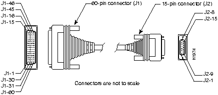
Table A-11 : X.21 DTE Cable Pinouts (DB-60 to DB-15)
J1-48
J1-47
|
GND
MODE_2
|
Shorting Group
|
-
|
--
|
--
|
J1-51
J1-52
|
GND
MODE_DCE
|
Shorting Group
|
--
|
--
|
--
|
| J1-46
|
Shield_GND
|
Single
|
--
|
J2-1
|
Shield GND
|
J1-11
J1-12
|
TxD/RxD+
TxD/RxD--
|
Twisted pair no. 3
|
--->
--->
|
J2-2
J2-9
|
Transmit+
Transmit--
|
J1-9
J1-10
|
RTS/CTS+
RTS/CTS--
|
Twisted pair no. 2
|
--->
--->
|
J2-3
J2-10
|
Control+
Control--
|
J1-28
J1-27
|
RxD/TxD+
RxD/TxD--
|
Twisted pair no. 6
|
<---
<---
|
J2-4
J2-11
|
Receive+
Receive--
|
J1-1
J1-2
|
CTS/RTS+
CTS/RTS--
|
Twisted pair no. 1
|
<---
<---
|
J2-5
J2-12
|
Indication+
Indication--
|
J1-26
J1-25
|
RxC/TxCE+
RxC/TxCE--
|
Twisted pair no. 5
|
<---
<---
|
J2-6
J2-13
|
Timing+
Timing--
|
J1-15
Shield
|
Control_GND
--
|
Twisted pair no. 4
|
--
--
|
J2-8
Shield
|
Control GND
--
|
1 Any pin not referenced is not connected.
Table A-12 : X.21 DCE Cable Pinouts (DB-60 to DB-15)
J1-48
J1-47
|
GND
MODE_2
|
Shorting Group
|
--
|
--
|
--
|
| J1-46
|
Shield_GND
|
Single
|
--
|
J2-1
|
Shield GND
|
J1-28
J1-27
|
RxD/TxD+
RxD/TxD--
|
Twisted pair no. 6
|
<---
<---
|
J2-2
J2-9
|
Transmit+
Transmit--
|
J1-1
J1-2
|
CTS/RTS+
CTS/RTS--
|
Twisted pair no. 1
|
<---
<---
|
J2-3
J2-10
|
Control+
Control--
|
J1-11
J1-12
|
TxD/RxD+
TxD/RxD--
|
Twisted pair no. 3
|
--->
--->
|
J2-4
J2-11
|
Receive+
Receive--
|
J1-9
J1-10
|
RTS/CTS+
RTS/CTS--
|
Twisted pair no. 2
|
--->
--->
|
J2-5
J2-12
|
Indication+
Indication--
|
J1-24
J1-23
|
TxC/RxC+
TxC/RxC--
|
Twisted pair no. 4
|
--->
--->
|
J2-6
J2-13
|
Timing+
Timing--
|
J1-15
Shield
|
Control_GND
--
|
Twisted pair no. 5
|
--
--
|
J2-8
Shield
|
Control GND
--
|
1 Any pin not referenced is not connected.
Ethernet Cable Assembly and Pinouts
Figure A-6 shows an Ethernet (AUI) cable assembly, and Table A-13 lists an AUI cable pinouts.
Figure A-6 : Ethernet (AUI) Cable Assembly
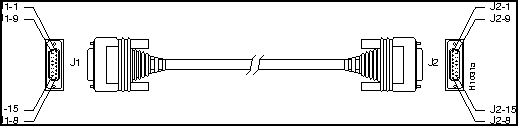
Table A-13 : Ethernet (AUI) Cable Pinouts (DB-15)
| 3
|
DO-A
|
Data Out Circuit A
|
| 10
|
DO-B
|
Data Out Circuit B
|
| 11
|
DO-S
|
Data Out Circuit Shield
|
| 5
|
DI-A
|
Data In Circuit A
|
| 12
|
DI-B
|
Data In Circuit B
|
| 4
|
DI-S
|
Data In Circuit Shield
|
| 2
|
CI-A
|
Control In Circuit A
|
| 9
|
CI-B
|
Control In Circuit B
|
| 1
|
CI-S
|
Control In Circuit Shield
|
| 6
|
VC
|
Voltage Common
|
| 13
|
VP
|
Voltage Plus
|
| 14
|
VS
|
Voltage Shield (L25 and M25)
|
| Shell
|
PG
|
Protective Ground
|
1 Any pin not referenced is not connected.
Token Ring Pinouts
The pinouts for the Token Ring interface port is in Table A-14.
Table A-14 : Token Ring Port Pinouts (DB-9)
| 1
|
Receive
|
| 3
|
+5V2
|
| 5
|
Transmit
|
| 6
|
Receive
|
| 9
|
Transmit
|
1 Pins 2, 4, 7, and 8 are ground.
2 600 mA maximum.
Asynchronous Serial Ports
Figure A-7 shows the RJ-45 breakout cable with pinouts for the 68-pin SCSI port and the RJ-45 serial port. Table A-15 contains the pinouts for the RJ-45 end, and Table A-16 contains the pinouts for the 68-pin SCSI type connector. Refer to the section "RJ-45 Adapter Pinouts" for cable and adapter configurations that can be used to connect terminals and modems to Cisco 2500 series products.
Figure A-7 : Asynchronous Serial Interface Breakout Cable Assembly
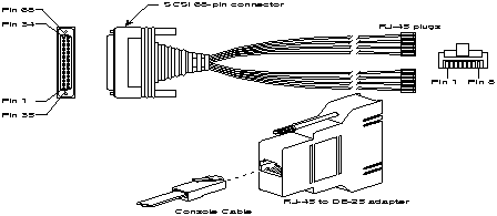
Table A-15 : Asynchronous Breakout Cable Pinouts (8-Pin RJ-45)
| 1
|
CTS
|
<---
|
| 2
|
DSR/DCD
|
<---
|
| 3
|
RXD
|
<---
|
| 4
|
GND
|
-
|
| 5
|
GND
|
-
|
| 6
|
TXD
|
--->
|
| 7
|
DTR
|
--->
|
| 8
|
RTS
|
--->
|
Table A-16 : Asynchronous Breakout Cable Pinouts (68-Pin SCSI)
| 1
|
8
|
RTS
|
2
|
|
|
7
|
DTR
|
36
|
|
|
6
|
TXD
|
3
|
|
|
5
|
TXD GND
|
37
|
|
|
4
|
RXD GND
|
4
|
|
|
3
|
RXD
|
38
|
|
|
2
|
DSR
|
5
|
|
|
1
|
CTS
|
39
|
| 2
|
8
|
RTS
|
6
|
|
|
7
|
DTR
|
40
|
|
|
6
|
TXD
|
7
|
|
|
5
|
TXD GND
|
41
|
|
|
4
|
RXD GND
|
8
|
|
|
3
|
RXD
|
42
|
|
|
2
|
DSR
|
9
|
|
|
1
|
CTS
|
43
|
| 3
|
8
|
RTS
|
10
|
|
|
7
|
DTR
|
44
|
|
|
6
|
TXD
|
11
|
|
|
5
|
TXD GND
|
45
|
|
|
4
|
RXD GND
|
12
|
|
|
3
|
RXD
|
46
|
|
|
2
|
DSR
|
13
|
|
|
1
|
CTS
|
47
|
| 4
|
8
|
RTS
|
14
|
|
|
7
|
DTR
|
48
|
|
|
6
|
TXD
|
15
|
|
|
5
|
TXD GND
|
49
|
|
|
4
|
RXD GND
|
16
|
|
|
3
|
RXD
|
50
|
|
|
2
|
DSR
|
17
|
|
|
1
|
CTS
|
51
|
| 5
|
8
|
RTS
|
18
|
|
|
7
|
DTR
|
52
|
|
|
6
|
TXD
|
19
|
|
|
5
|
TXD GND
|
53
|
|
|
4
|
RXD GND
|
20
|
|
|
3
|
RXD
|
54
|
|
|
2
|
DSR
|
21
|
|
|
1
|
CTS
|
55
|
| 6
|
8
|
RTS
|
22
|
|
|
7
|
DTR
|
56
|
|
|
6
|
TXD
|
23
|
|
|
5
|
TXD GND
|
57
|
|
|
4
|
RXD GND
|
24
|
|
|
3
|
RXD
|
58
|
|
|
2
|
DSR
|
25
|
|
|
1
|
CTS
|
59
|
| 7
|
8
|
RTS
|
26
|
|
|
7
|
DTR
|
60
|
|
|
6
|
TXD
|
27
|
|
|
5
|
TXD GND
|
61
|
|
|
4
|
RXD GND
|
28
|
|
|
3
|
RXD
|
62
|
|
|
2
|
DSR
|
29
|
|
|
1
|
CTS
|
63
|
| 8
|
8
|
RTS
|
30
|
|
|
7
|
DTR
|
64
|
|
|
6
|
TXD
|
31
|
|
|
5
|
TXD GND
|
65
|
|
|
4
|
RXD GND
|
32
|
|
|
3
|
RXD
|
66
|
|
|
2
|
DSR
|
33
|
|
|
1
|
CTS
|
67
|
Figure A-8 shows the DB-25 breakout cable with pinouts for the 68-pin port and the DB-25 port. Table A-17 lists the pinouts for the DB-25 end, and Table A-18 lists the pinouts for the 68-pin connector end.
Figure A-8 : Asynchronous Serial Interface Breakout Cable Assembly (68-Pin to DB-25)
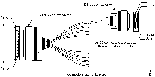
Table A-17 : Asynchronous Breakout Cable Pinouts (DB-25)
| 4
|
RTS
|
--->
|
| 20
|
DTR
|
--->
|
| 2
|
TXD
|
--->
|
| 7
|
TXD GND
|
---
|
| 7
|
RXD GND
|
---
|
| 3
|
RXD
|
<---
|
| 8
|
DSR
|
<---
|
| 5
|
CTS
|
<---
|
1 Any pin not referenced is not connected.
Table A-18 : Asynchronous Cable Pinouts (68-Pin to DB-25)
| 1
|
4
|
RTS
|
2
|
|
|
20
|
DTR
|
36
|
|
|
2
|
TXD
|
3
|
|
|
7
|
TXD GND
|
37
|
|
|
7
|
RXD GND
|
4
|
|
|
3
|
RXD
|
38
|
|
|
8
|
DSR
|
5
|
|
|
5
|
CTS
|
39
|
| 2
|
4
|
RTS
|
6
|
|
|
20
|
DTR
|
40
|
|
|
2
|
TXD
|
7
|
|
|
7
|
TXD GND
|
41
|
|
|
7
|
RXD GND
|
8
|
|
|
3
|
RXD
|
42
|
|
|
8
|
DSR
|
9
|
|
|
5
|
CTS
|
43
|
| 3
|
4
|
RTS
|
10
|
|
|
20
|
DTR
|
44
|
|
|
2
|
TXD
|
11
|
|
|
7
|
TXD GND
|
45
|
|
|
7
|
RXD GND
|
12
|
|
|
3
|
RXD
|
46
|
|
|
8
|
DSR
|
13
|
|
|
5
|
CTS
|
47
|
| 4
|
4
|
RTS
|
14
|
|
|
20
|
DTR
|
48
|
|
|
2
|
TXD
|
15
|
|
|
7
|
TXD GND
|
49
|
|
|
7
|
RXD GND
|
16
|
|
|
3
|
RXD
|
50
|
|
|
8
|
DSR
|
17
|
|
|
5
|
CTS
|
51
|
| 5
|
4
|
RTS
|
18
|
|
|
20
|
DTR
|
52
|
|
|
2
|
TXD
|
19
|
|
|
7
|
TXD GND
|
53
|
|
|
7
|
RXD GND
|
20
|
|
|
3
|
RXD
|
54
|
|
|
8
|
DSR
|
21
|
|
|
5
|
CTS
|
55
|
| 6
|
4
|
RTS
|
22
|
|
|
20
|
DTR
|
56
|
|
|
2
|
TXD
|
23
|
|
|
7
|
TXD GND
|
57
|
|
|
7
|
RXD GND
|
24
|
|
|
3
|
RXD
|
58
|
|
|
8
|
DSR
|
25
|
|
|
5
|
CTS
|
59
|
| 7
|
4
|
RTS
|
26
|
|
|
20
|
DTR
|
60
|
|
|
2
|
TXD
|
27
|
|
|
7
|
TXD GND
|
61
|
|
|
7
|
RXD GND
|
28
|
|
|
3
|
RXD
|
62
|
|
|
8
|
DSR
|
29
|
|
|
5
|
CTS
|
63
|
| 8
|
4
|
RTS
|
30
|
|
|
20
|
DTR
|
64
|
|
|
2
|
TXD
|
31
|
|
|
7
|
TXD GND
|
65
|
|
|
7
|
RXD GND
|
32
|
|
|
3
|
RXD
|
66
|
|
|
8
|
DSR
|
33
|
|
|
5
|
CTS
|
67
|
RJ-45 Ethernet Pinouts
Table A-19 lists the pinouts for an Ethernet based RJ-45, and Table A-20 lists pinouts for the Ethernet on a model 2505 or model 2507.
Table A-19 : Ethernet 10BaseT (RJ-45) Port Pinouts
| 1
|
TX+
|
| 2
|
TX--
|
| 3
|
RX+
|
| 4
|
---
|
| 5
|
---
|
| 6
|
RX--
|
| 7
|
---
|
| 8
|
---
|
1 Any pin not referenced on a connector is not connected.
Table A-20 : Ethernet 10BaseT Port Pinouts (For 2505 and 2507 Models)
| 1
|
RX+
|
| 2
|
RX--
|
| 3
|
TX+
|
| 6
|
TX--
|
RJ-45 Adapter Pinouts
Refer to Table A-21 for a list of the pins used on the RJ-45 connector, the male/female DTE adapter., the male/female DCE adapter, and the male modem adapter used to connect terminals and modems to Cisco 2500 series products. The connection of pins between the RJ-45 connector and the end device depends on the type of cable used, either straight or rolled. A straight cable connects pin 1 to pin 1, pin 2 to pin 2, and so on. A rolled cable connects pin 1 to pin 8, pin 2 to pin 7, and so on. Cisco 2500 Series products now ship with a rolled cable. Refer to Table A-22 for the cable and adapter configurations that can be used to connect terminals and modems to Cisco 2500 series products. Table A-23 and Table A-24list the suggested adapter pinouts.
Table A-21 : Pins for the RJ-45, M/F DTE, M/F DCE, and MMOD
| 1
|
4
|
5
|
5
|
| 2
|
20
|
6
|
8
|
| 3
|
2
|
3
|
3
|
| 4
|
7
|
7
|
7
|
| 5
|
7
|
7
|
7
|
| 6
|
3
|
2
|
2
|
| 7
|
6
|
20
|
20
|
| 8
|
5
|
4
|
4
|
1 The FDTE adapter that is available through Cisco is labeled "Terminal."
2 The MMOD adapter that is available through Cisco is labeled "Modem."
Table A-22 : Connection Configuration
| Console/aux
|
Rolled1
|
FDTE
|
Terminal
|
| Console/aux
|
Straight
|
FDCE
|
Terminal
|
| Console/aux
|
Rolled1
|
MDCE2
|
Modem
|
| Console/aux
|
Straight
|
MDTE2
|
Modem
|
| Aux/console
|
Rolled1
|
MMOD
|
Modem
|
1 An octal cable or RJ-45 breakout cable is equivalent to a rolled cable.
2 Modify the adapter by removing DB-25 pin 6 and placing it into the pin 8 position.
Table A-23 lists suggested DB-25 to DB-9 adapter pinouts.
Table A-23 : DB-25 to DB-9 Adapter Pinouts
| 2
|
TXD
|
3
|
| 3
|
RXD
|
2
|
| 4
|
RTS
|
7
|
| 5
|
CTS
|
8
|
| 6
|
DSR
|
6
|
| 8
|
DCD
|
1
|
| 20
|
DTR
|
4
|
Table A-24 lists suggested RJ-45-to-DB-9 adapter pinouts.
Table A-24 : RJ-45 to DB-9 Adapter Pinouts
| 1
|
RTS
|
7
|
| 2
|
DTR
|
4
|
| 3
|
TXD
|
3
|
| 4
|
GND
|
5
|
| 5
|
GND
|
5
|
| 6
|
RXD
|
2
|
| 7
|
DSR
|
6
|
| 8
|
CTS
|
8
|
Copyright 1988-1996 © Cisco Systems Inc.
