|
|

This chapter discusses maintenance of the chassis and its components. As your internetworking requirements change over time, use this information to adapt as needed. Certain cards and appliques can be configured for different internetworking functions. This chapter discusses these configuration requirements.
If any upgrades requiring card, microcode, or software replacement are necessary, the appropriate documentation called configuration notes will be shipped with the replacement parts or upgrades you order.
This chapter contains information on the following:
![]()
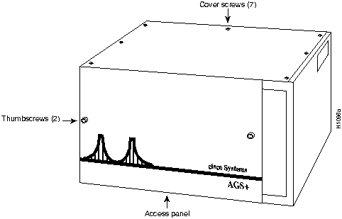
Access to the chassis interior requires that you remove the front panel to access the cards or the top cover to access the rest of the chassis components. The following procedure includes instructions for both.
The following tools are required for accessing the chassis interior:
Following is the procedure for accessing the chassis interior.
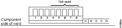
Figure 5-1 : Chassis Front and Top Panels Some cards can be configured for different user applications. For example, the CSC-MCI card has jumpers that allow you to change from data terminal equipment (DTE) mode to data communications equipment (DCE) mode depending upon your requirements. In addition, most Multibus cards have card-numbering switches that allow you to reconfigure them for different slot positions in the chassis.
Included in this section is an illustration of each card and tables showing its configurable jumpers and switches. Following is a listing of all the configurable cards in the chassis. Cards excluded from this list are not configurable through hardware alterations.
Most Multibus interface cards require that unique card numbers be assigned to them before the entire system becomes operational. Cards that are installed in the chassis are correctly numbered before shipment, but you may have to renumber them when you order and install new or additional cards.
These card numbers are position markers for the system software that let the system know what cards are installed in what slots. The card numbers are assigned by way of a dual in-line package (DIP) switch located on the component side of the card. These switches are set so that each card has a unique card number. In general, each card number should be unique within the set of all cards installed in the chassis. Exceptions to this are the ENVM and processor cards, which have no switches and are always installed in the same two slots (the top slot and the second slot from the top, respectively).
Processor Card Configuration Register
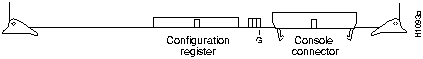
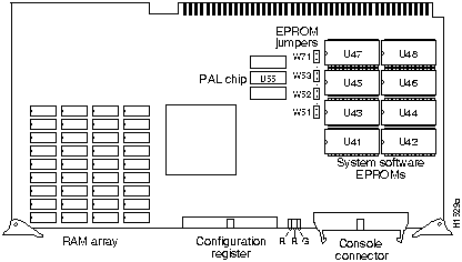
For both the CSC/3 and CSC/4 processor cards, the 50-pin header in the center of the front edge of the card is used as a configuration register for processor functions and diagnostics. The following section describes the settings for this register. Figure 5-2 shows a partial component-side view of the processor cards. Both cards contain the same components and basic physical layout as illustrated.
Figure 5-2 : CSC/3 and CSC/4 Processor Cards---Partial Component-Side View Configuration Register Settings
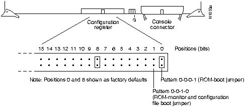
The processor cards have a 16-bit hardware configuration register: the far right 16 pairs of jumper pins on the 50-pin header in the center of the card. (Refer to Figure 5-3.) Bit 0 (or position 0) is the far right vertical pair of pins. To set a bit to 1, insert a vertical jumper. To clear a bit to 0, remove the vertical jumper. Figure 5-3 shows the configuration register with the factory settings for the CSC/3 and CSC/4.
Figure 5-3 : CSC/3 and CSC/4 Configuration Register To change configuration register settings, turn off the system, set or clear the bits by inserting or removing jumpers, and restart the system (or change the jumper settings while the power is still on, and then give the privileged command reload). It is not necessary to remove the processor card from the backplane or to turn off the power to change a jumper setting.
The lowest four bits of the processor configuration register (bits 3, 2, 1, and 0) form the boot field. The boot field specifies a number in binary. If you set the boot field value to 0, you must boot the operating system manually by giving a b (or boot) command to the system bootstrap program. If you set the boot field value to 1 (the factory default), the system boots using the default ROM software. If you set the boot field to any other bit pattern, the boot system commands override the default boot filenames when netbooting. For example, a jumper configuration of 0-0-1-0 (bits 3 through 0) is used when using the boot system flash command with the Flash memory card.
The system creates a boot filename as part of the automatic configuration processes. To form the boot filename, the system starts with cisco and links the octal equivalent of the boot field number, a dash, and the processor type name. Table 5-1 lists the default boot filenames or actions for the CSC/4 processor. The list is the same for the CSC/3 processor card; however, csc3 is substituted for csc4.
Table 5-1 : Default Boot Filenames---Boot Field Jumpers
Bit 8 in the configuration register controls the console Break key. Setting bit 8 to 1 (the factory default) causes the processor to ignore the console Break key. Clearing bit 8 to 0 causes the processor to interpret Break as a command to force the system into the bootstrap monitor, suspending normal operation.
Bit 9 in the configuration register controls the use of a secondary bootstrap procedure when netbooting. If this bit is set to 1, a secondary bootstrap (with the filename boot-csc4 [or csc3]) is first loaded into the system over the network. This bootstrap image then loads in the desired boot file, completing the netbooting process.
Bit 10 in the configuration register controls the host portion of the Internet broadcast address. Setting bit 10 causes the processor to use all zeros; clearing bit 10 (the factory default) causes the processor to use all ones. Bit 10 interacts with bit 14, which controls the network and subnet portions of the broadcast address. Table 5-2 shows the combined effect of bits 10 and 14. This effect is overridden by values set in NVRAM using the ip broadcast address command.
Table 5-2 : Configuration Register Settings for Broadcast Address Destination
Setting the Console Port Baud Rate
Bits 11 and 12 in the configuration register determine the baud rate of the console port. Table 5-3 shows the bit settings for the four available baud rates. (The factory default is 9600 baud.)
Table 5-3 : System Console Port Baud Rate Settings
General Configuration Register Settings
Bit 13 in the configuration register determines the system response to a boot-load failure. Setting
Bit 14 in the configuration register controls the network and subnet portions of the Internet broadcast address. Setting bit 14 causes the system to include the network and subnet portions of its address in the broadcast address. Clearing bit 14 causes the system to set the entire broadcast address to all ones or all zeros, depending on the setting of bit 10. By factory default, bit 14 is cleared to 0. See Table 5-2 for the combined effect of bits 10 and 14.
Bit 15 in the configuration register controls the factory diagnostic mode in the system. Setting bit 15 causes the system to produce detailed CPU self-check messages, to automatically prompt for interface addresses (not look for them on the network), to not read configuration files or NVRAM, and to automatically set to diagnostic tracing modes using the debug commands. Clearing bit 15 (the factory default) causes the system to operate normally. Bit 15 is also used for password recovery.
Bits 16 through 19 and bit 24 are not currently used.
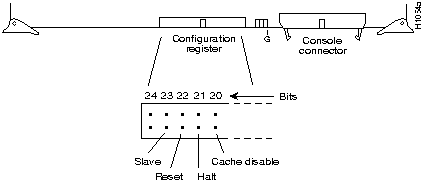
Bits 20 through 23 (the four pairs of pins toward the far left of the 50-pin header) are not used in normal operation; however, they can be used to invoke the Slave mode, External Reset function, Halt Processor, and Cache Disable mode functions (respectively) on any processor card.
Figure 5-4, which shows the optional jumper configurations, represents a partial front-edge view of the configuration register on a processor card installed in the card cage.
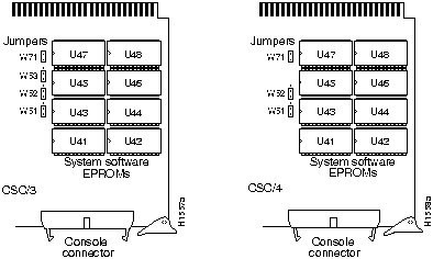
Figure 5-4 : CSC/3 and CSC/4 Optional Configuration Register Settings The CSC/3 and CSC/4 processor cards have configurable jumpers that control critical memory functions for the different sizes of erasable programmable read-only memories (EPROMs) that can be installed. These jumpers are changed only when the EPROM memory sizes are changed. Do not change these jumpers from their default settings unless you are instructed to do so when the software is changed. Figure 5-5 shows the positions of jumpers W51 through W53 on the CSC/3 card (left side) and jumpers W51 through W52 on the CSC/4 card (right side).
Figure 5-5 : CSC/3 and CSC/4 EPROM Jumper Locations---Partial Component-Side Views
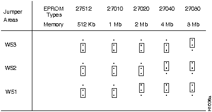
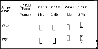
Figure 5-6 and Figure 5-7 show the EPROM jumper settings for the CSC/3 and CSC/4 cards, respectively.
Figure 5-6 : CSC/3 EPROM Jumper Settings Figure 5-7 : CSC/4 EPROM Jumper Settings
Configuring the CSC-MCI and CSC-SCI Cards
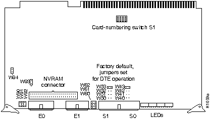
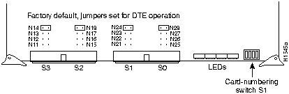
The following sections discuss the various configuration changes that can be made to the CSC-MCI and CSC-SCI cards. For both cards, card numbers are assigned by setting a dual in-line package (DIP) switch (S1). For the MCI card, the card-numbering switch (S1) is located toward the back of the card near the bus edge connector. (See Figure 5-8.) For the SCI card, the card-numbering switch (S1) is located toward the right-front edge of the card. (See Figure 5-9.)
Figure 5-8 : MCI Card Jumpers and Switches---Component-Side View Figure 5-9 : SCI Card Jumpers and Switches---Partial Component-Side View
CSC-MCI and CSC-SCI Card Numbering
Table 5-4 shows the switch (S1) settings for card numbering the MCI and SCI cards. The card numbers within the set of MCI and SCI cards installed in the chassis must be unique. These card numbers must also be unique among the other cards installed. Card number 0 can be used only if no ciscoBus controller card is installed; the ciscoBus controller card is card number 0 by default.
Table 5-4 : CSC-MCI and CSC-SCI Switch (S1) Settings for Card Numbering
CSC-MCI and CSC-SCI Mode and Clocking Options
On the MCI card, jumpers W51 and W41 control the serial ports 0 and 1 in data communications equipment (DCE) mode. On the SCI card, jumpers N22, N26, N12, and N16 control the serial ports 0 through 3 in DCE mode. In addition to changing these jumpers for DCE operation, you must configure the clock rate on each serial interface of the interface card using the clockrate speed interface subcommand (where speed is the bit rate of the interface in bits per second [bps]). The applique must be DCE (or configured as DCE) to generate the clock signals.
Following is sample output of the clockrate speed command:
1200, 2400, 4800, 9600, 19200, 38400, 56000, 6400, 7200, 12500, 148000, 500000, 800000, 1000000, 1300000, 2000000, and 4000000
The fastest speeds might not work if your cable is too long. Speeds faster than 148 kbps are not recommended for RS-232 or RS-232 SDLC signaling. It is recommended that you use the RS-232 and SDLC appliques only at speeds up to 64 kbps; for speeds above this, use RS-449, X.21, or HD V.35.
Most DTE interfaces require a Normal External Transmit Clock signal. All DCE interfaces require an Internal Transmit Clock (noninverted) signal. The MCI card clocking options are controlled by jumper areas W40 through W53, and the SCI card clocking options are controlled by jumper areas N11 through N28.
Occasionally, delays occur between the Serial Clock Transmit External (SCTE) clock and the transmitted data that may push the data transition out to the point where using an inverted clock is appropriate (jumpers W42 and W52 for the MCI and N13, N17, N23, and N27 for the SCI); however, an inverted clock is not recommended.
Typical delays indicate that the inverted clock may be appropriate above 1.3 megabits per
Table 5-5 and Table 5-6 show the jumper settings for the MCI and SCI clock options, respectively. The last two columns of these tables (DTE and DCE) indicate the setting that should be used with either a DTE or DCE applique. Unless specifically noted, all products are shipped with the factory default setting to work with the DTE applique, which requires external clocking; the channel service unit/digital service unit (CSU/DSU) provides the clocking for the circuit.
Table 5-5 : CSC-MCI Jumper Settings for Clock Options
Table 5-6 : CSC-SCI Jumper Settings for Clock Options
The CSC-MCI card provides up to two Ethernet ports (the SCI card has none) and uses grounding options to accommodate the differences between the Ethernet Version 1 and IEEE 802.3 electrical specifications. Ethernet Version 1 permits certain signals to float, whereas IEEE 802.3 requires the signals to be grounded. Table 5-7 lists the CSC-MCI grounding options. Inserting a jumper grounds the signal and removing a jumper allows the signal to float. The factory default is to ground all signal pairs, which is compatible with both Ethernet and IEEE 802.3 requirements.
Table 5-7 : CSC-MCI Jumper Settings for Grounding Options
On the MCI card, jumpers W94 and W93 are 3-pin jumpers that select between Ethernet and
Configuring the CSC-MEC and CSC-C2MEC Cards
Figure 5-10 shows the appropriate jumper settings (jumpers W1 through W6) to use when you attach Ethernet Version 1 cables to the Ethernet connector. Figure 5-11 shows the appropriate jumper settings to use when you attach Ethernet Version 2 and IEEE 802.3 cables. ( Jumper settings shown in Figure 5-11are factory defaults.) The explanation for the Ethernet jumper settings follows.
Figure 5-10 : Jumper Settings for Ethernet Version 1 Figure 5-11 : Jumper Settings for Ethernet Version 2 and IEEE 802.3
Jumpers on pin sets W1 through W6 set the electrical specifications for the Ethernet transceiver connection. Each jumper is moved over one pin (compare the jumpers in Figure 5-10 and
Configuring CSC-1R, CSC-2R, and CSC-C2CTR Token Ring Cards
The following sections discuss the configuration requirements for the CSC-1R, CSC-2R, and CSC-C2CTR.
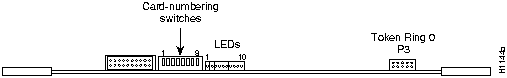
CSC-1R and CSC-2R Card Numbering
Switches 1 through 3 on the front edge of the CSC-1R and CSC-2R cards (see Figure 5-12) control card numbering within the chassis. (Switches 4 through 8 have no function.) Configure the switches on the CSC-1R and CSC-2R cards to select the desired card number. These switches (1 through 3) are listed in Table 5-8 from left to right when viewing the front edge of the card. Only the CSC-1R card is shown; the CSC-2R card numbering switches are in the same order and position on the card and have the same function. Switches 4 through 8 should all be down (off).
Figure 5-12 : CSC-1R and CSC-2R Card-Numbering Switches---Front-Edge View The card numbers of each card within a certain type (Token Ring and so forth) must be unique to allow the system to distinguish between multiple cards of one type. For example, if two CSC-1R cards are installed, they should be numbered Card 0 and Card 1. If one CSC-R16M card and one CSC-1R card are installed, they should also be Card 0 and Card 1. All other card-numbering fundamentals apply. Table 5-8 lists the card-numbering scheme for the CSC-1R and CSC-2R cards.
Table 5-8 : CSC-1R and CSC-2R Card-Numbering Switch Settings
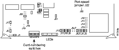
Selecting CSC-1R and CSC-2R Token Ring Port Speed
The speed of the Token Ring ports on the CSC-1R and CSC-2R cards must be configured immediately after the first reboot (following installation) using either the configuration dialog routine, the config terminal command, or the setup command.
The speed of the ports on these cards must be configured by the user; there is no factory default for port speed. The ports are independent and can be configured for two different speeds. Following is sample output of how to configure both ports on the CSC-2R Token Ring card for 16 megabits per second (Mbps) using the config terminal command:
Selecting CSC-C2CTR Token Ring Port Speed
The speed of the ciscoBus Token Ring ports on the CSC-C2CTR card must be configured immediately after first reboot (following installation). In the following sample configuration, a new ciscoBus Token Ring interface is assigned a ring speed of 16 megabits per second (Mbps) and an IP address using the configure terminal command from the terminal. The configuration is then written to configuration memory using the write memory command.
The following steps provide instructions for a basic configuration: enabling an interface, setting the ring speed, and specifying IP routing. You may also need to enter other configuration subcommands, depending upon the requirements for your system configuration. (Configuration subcommands are described in the router products configuration publication.) Refer to the previous example as necessary.
In the following example, press Return after each command line.
Configuring the CSC-R16M Token Ring Card
The following sections discuss the configuration requirements of the CSC-R16M card.
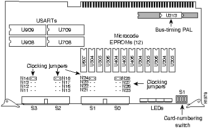
The card number of the CSC-R16M is selected through the use of software-readable dual in-line package (DIP) switches on the front edge of the card. Only switches 1 through 3 are used; all others are set to down (or off). Figure 5-13 shows these switches on the card front edge as viewed from left to right. The card number of each card within a certain type (Token Ring and so forth) must be unique to allow the system to distinguish between multiple cards of one type. For example, if two CSC-R16M cards are installed, they should be numbered Card 0 and Card 1. If one CSC-R16M card and one CSC-1R card are installed, they also should be Card 0 and Card 1. Table 5-9 lists the card-numbering scheme for the CSC-R16M. All other card-numbering fundamentals apply.
Figure 5-13 : CSC-R16M Card-Numbering Switches---Partial Front-Edge View Table 5-9 : CSC-R16M Card-Numbering Switch Settings
Selecting CSC-R16M Token Ring Port Speed
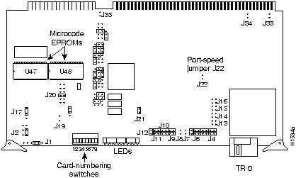
The port speed of the CSC-R16M card is jumper configurable. Jumper area J22 configures the CSC-R16M for either 4-megabits per second (Mbps) or 16-Mbps operation. (See Figure 5-14.) No jumper at jumper area J22 (the factory default setting) selects 16-Mbps operation, while installing a jumper at location J22 selects 4-Mbps operation. The spare jumper to use at J22 is placed on the posts at jumper area J21. CSC-R16M cards are shipped configured to run at 16 Mbps (J22 has no jumper). To install the J22 jumper, remove the jumper from J21.
Figure 5-14 : CSC-R16M Jumper and Switch Positions The chassis uses the 400W model MAS-400 or MAS-400B power supply. In the United Kingdom, the chassis uses the 400W model MAS-25 power supply. If you determine that you have a power supply problem, contact a customer service representative. Before calling, verify the input voltage of your system by checking the label next to the power switch on the rear of the chassis and have the following information available:
The chassis uses the model MAS-10 or MAS-10B blower vent assemblies for system cooling. In the United Kingdom, the chassis uses the MAS-10B exclusively. If you determine that you have a cooling system problem, contact a customer service representative. Before calling, verify the input voltage of your system and have the following information available:
Following are illustrations of all of the interface, processor, and controller cards that can be used in the chassis. Use these illustrations to locate software and microcode EPROMs, connectors, jumpers, and switches on the cards in your chassis. Cards with the designator (C2) can be used with either the CSC-CCTL card or the CSC-CCTL2 card, and cards with the C2 designator can only be used with the CSC-CCTL2 card. (For more information, refer to Table 1-3 in Chapter 1.)
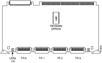
Figure 5-15 : CSC-1R Token Ring Interface Card---Component-Side View
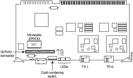
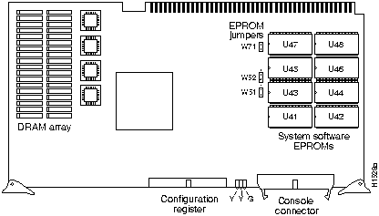
Figure 5-16 : CSC-2R Token Ring Interface Card---Component-Side View Figure 5-17 : CSC/3 Processor Card---Component-Side View
Figure 5-18 : CSC/4 Processor Card---Component-Side View Figure 5-19 : CSC-C2CTR ciscoBus Token Ring Interface Card---Component-Side View
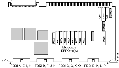
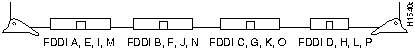
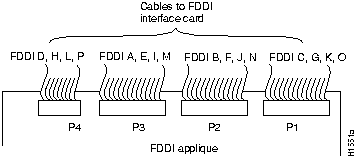
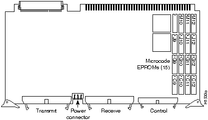
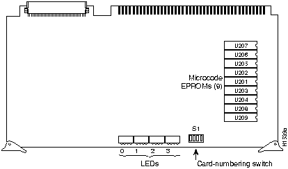
Figure 5-20 : CSC-(C2)FCI FDDI Interface Card---Component-Side View Figure 5-21 : CSC-C2FCIT FDDI Interface Card---Component-Side View Figure 5-22 : FDDI Applique Cables to FDDI Card Connectors---Partial Component-Side View
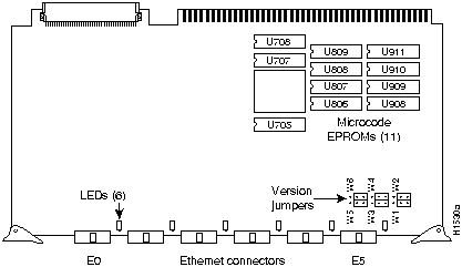
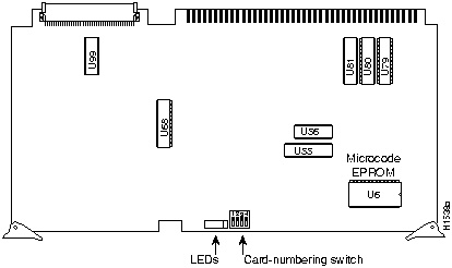
Figure 5-23 : CSC-(C2)HSCI High-Speed Serial Interface (HSSI) Card---Component-Side View Figure 5-24 : CSC-(C2)MEC6 Ethernet Interface Card---Component-Side View Figure 5-25 : CSC-CCTL ciscoBus Controller Card---Component-Side View Figure 5-26 : CSC-CCTL2 ciscoBus2 Controller Card---Component-Side View
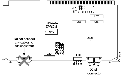
Figure 5-27 : CSC-ENVM Environmental Monitor Card---Component-Side View The new CSC-ENVM card installed in your AGS+ chassis (or received as a spare) uses nonvolatile random-access memory (NVRAM) devices with built-in lithium batteries. These combination NVRAM/battery devices replace the multiple NVRAM devices and three separate nickel-cadmium batteries on previous CSC-ENVM cards; otherwise, the CSC-ENVM cards are identical. The three spaces in the CSC-ENVM card are where the nickel-cadmium batteries were installed, and are intentionally left empty. The performance and memory capacity of both cards is the same in every respect.
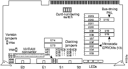
Figure 5-28 : CSC-MCI Multiport Communications Interface Card---Component-Side View The designator CSC-MCI includes three different physical versions of the card: (1) two Ethernet connectors, (2) one Ethernet connector and one serial connector, (3) two Ethernet connectors and two serial connectors.
One or the other of these three physical versions is used for the following interface combinations:
All three physical versions of the CSC-MCI card have the 50-pin NVRAM connector for the CSC-MC memory card and the CSC-MC+ Flash memory card.
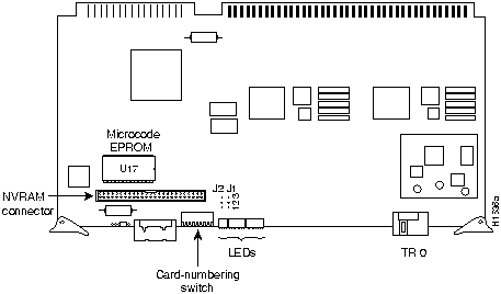
Figure 5-29 : CSC-R16M Token Ring Interface Card---Component-Side View Figure 5-30 : CSC-SCI Serial Communications Interface Card---Component-Side View The designator CSC-SCI includes the CSC-4S, CSC-4T, and CSC-2S2T cards.
Copyright 1988-1996 © Cisco Systems Inc.
![]()
Action/Filename
Bit 3
Bit 2
Bit 1
Bit 0
bootstrap mode
0
0
0
0
ROM software
0
0
0
1
cisco2-csc4
0
0
1
0
cisco3-csc4
0
0
1
1
cisco4-csc4
0
1
0
0
cisco5-csc4
0
1
0
1
cisco6-csc4
0
1
1
0
cisco7-csc4
0
1
1
1
cisco10-csc4
1
0
0
0
cisco11-csc4
1
0
0
1
cisco12-csc4
1
0
1
0
cisco13-csc4
1
0
1
1
cisco14-csc4
1
1
0
0
cisco15-csc4
1
1
0
1
cisco16-csc4
1
1
1
0
cisco17-csc4
1
1
1
1
Bit 14
Bit 10
Address (<net><host>)
out
out
<ones><ones>
out
in
<zeros><zeros>
in
in
<net><zeros>
in
out
<net><ones>
Baud
Bit 12
Bit 11
96001
0
0
4800
0
1
1200
1
0
2400
1
1
1 Factory default
bit 13 causes the system to load operating software from read-only memory (ROM) after five unsuccessful attempts to load a boot file from the network. Clearing bit 13 causes the system to continue attempting to load a boot file from the network indefinitely. By factory default, bit 13 is cleared to 0.
Card No.
S1-1
S1-2
S1-3
S1-4
01
Off
Off
Off
Off
1
Off
Off
Off
On
2
Off
Off
On
Off
3
Off
Off
On
On
4
Off
On
Off
Off
5
Off
On
Off
On
6
Off
On
On
Off
7
Off
On
On
On
1 Use only if no ciscoBus controller card is installed. The ciscoBus controller card is card number 0 by default.
Router# configure terminal
Enter configuration commands, one per line.
Edit with DELETE, CRTL/W, and CRTL/U;end with CTRL/Z
interface serial 0
clockrate 64000
^Z
Router# write memory
[ok]
Router#
The no clockrate command removes the clock rate if data terminal equipment (DTE) mode is desired. Refer to the appropriate configuration and reference publication for more information on these commands. Following are the acceptable clockrate speed settings, appearing as they are entered with the clockrate speed command:
second (Mbps), depending upon the DTE clock-to-data skews and setup required, and allowing some margin for temperature, cable, and other variables. Some DCE devices will not accept SCTE, so Serial Clock transmit (SCT) must be used. Inverting the clock may be the only way to compensate for the cable length and circuit delays in the DTE and DCE.
Jumper Pair
Signal Description
Interface
DTE
DCE
W53
Normal External Transmit Clock
Serial 0
X1
--
W52
Inverted External Transmit Clock
Serial 0
x
--
W51
Normal Internal Transmit Clock
Serial 0
--
X
W50
Inverted Internal Transmit Clock
Serial 0
--
x
W43
Normal External Transmit Clock
Serial 1
X1
--
W42
Inverted External Transmit Clock
Serial 1
x
--
W41
Normal Internal Transmit Clock
Serial 1
--
X
W40
Inverted Internal Transmit Clock
Serial 1
--
x
1 X = Recommended setting. x = Available but not recommended.
Jumper Pair
Signal Description
Interface
DTE
DCE
N 24
Normal External Transmit Clock
Serial 0
X1
--
N 23
Inverted External Transmit Clock
Serial 0
x
--
N 22
Normal Internal Transmit Clock
Serial 0
--
X
N 21
Inverted Internal Transmit Clock
Serial 0
--
x
N 28
Normal External Transmit Clock
Serial 1
X1
--
N 27
Inverted External Transmit Clock
Serial 1
x
--
N 26
Normal Internal Transmit Clock
Serial 1
--
X
N 25
Inverted Internal Transmit Clock
Serial 1
--
x
N 14
Normal External Transmit Clock
Serial 2
X1
--
N 13
Inverted External Transmit Clock
Serial 2
x
--
N 12
Normal Internal Transmit Clock
Serial 2
--
X
N 11
Inverted Internal Transmit Clock
Serial 2
--
x
N 18
Normal External Transmit Clock
Serial 3
X1
--
N 17
Inverted External Transmit Clock
Serial 3
x
--
N 16
Normal Internal Transmit Clock
Serial 3
--
X
N 15
Inverted Internal Transmit Clock
Serial 3
--
x
1 X = Recommended setting. x = Available but not recommended.
Jumper Pair
Signal Description
Interface
W90
Receive Pair Shield
First Ethernet
W91
Transmit Pair Shield
First Ethernet
W92
Power Pair Shield
First Ethernet
W60
Power Pair Shield
Second Ethernet
W61
Transmit Pair Shield
Second Ethernet
W62
Receive Pair Shield
Second Ethernet
IEEE 802.3 electrical levels. Jumper W94 controls the first Ethernet port, and jumper W93 controls the second Ethernet port. The factory default is to select IEEE 802.3 (Ethernet Version 2). Using the card orientation shown in Figure 5-8, place a jumper on the lower pair of pins to select Ethernet Version 1.
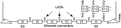
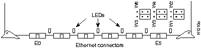
Figure 5-11) to change the electrical specifications of its corresponding connector (W1 for E0, and so forth). Pin set W1 corresponds to the far left connector (E0), using the orientation seen in
Figure 5-10 or Figure 5-11 (facing the component side of the card with the connectors at the bottom). Each connector corresponds consecutively to a pin set.
Card No.
Switch 11
Switch 2
Switch 3
0
Down2
Down
Down
1
Up
Down
Down
2
Down
Up
Down
3
Up
Up
Down
4
Down
Down
Up
5
Up
Down
Up
6
Down
Up
Up
1 Switches 4 through 8 have no function.
2 Down = Switch is off.
Router# configure terminal
Enter configuration commands, one per line.
Edit with DELETE, CRTL/W, and CRTL/U;end with CTRL/Z
interface tokenring 0
ring-speed 16
interface tokenring 1
ring-speed 16 (this line and the preceding line are not used for the CSC-1R)
^z
Router# write memory
[ok]
Router#
Port speed must equal ring speed. Failure to match the port speed to the ring speed can bring down the ring. The port inserts into the ring when you press Return after entering the command ring-speed 16. Only values of 4 or 16 Mbps will be accepted by the system because these are the only selectable speeds for the CSC-1R and CSC-2R ports.
![]()
Router# configure terminal
Enter configuration commands, one per line.
Edit with DELETE, CTRL/W, and CTRL/U; end with CTRL/Z
interface token ring n (n = the interface unit address 0, 1, 2, and so forth)
ring-speed 16
ip address 145.22.4.67 255.255.255.0
no shut
^z
Router# write memory
[ok]
router#
Failure to match the interface speed to the ring speed will bring down the ring. The speed of each interface on the CSC-C2CTR card must be configured to match the speed of the ring to which the interface is connected. Only values of 4 or 16 Mbps will be accepted by the system, and each interface on the CSC-C2CTR can be configured for either 4 or 16 Mbps.
![]()
the no shut command. After you enter no shut (or if the interface is already configured as up), the interface is inserted into the ring as soon as the Return key is pressed.
configure terminal
interface token ring n
ring-speed n
If IP routing is enabled on the system, you can assign an IP address and subnet mask to the interface with the ip address configuration subcommand as follows (where 111.111.111.111 and 255.255.255.0 represent the IP address and subnet mask, respectively):
ip address 111.111.111.111 255.255.255.0
Change the default shutdown state and bring the interface up by entering the following:
no shut
Specify the next Token Ring interface to configure by entering the following:
interface token ring 1
Repeat steps 3 through 6 for each new Token Ring interface.
press the z key).
write memory
The system will display an OK message to indicate that the configuration has been stored.
quit
This completes the procedure for selecting the port speed for the CSC-C2CTR Token Ring interface.
Card No.
Switch 11
Switch 2
Switch 3
0
Down2
Down
Down
1
Up
Down
Down
2
Down
Up
Down
3
Up
Up
Down
4
Down
Down
Up
5
Up
Down
Up
6
Down
Up
Up
1 Switches 4 through 8 have no function.
2 Down = Switch is off.
![]()
![]()
![]()
![]()
![]()
![]()
![]()
![]()
![]()