|
|

This appendix describes cable signals and pinouts.
The cables available from us meet FCC part 15J Class B requirements. When constructing your own cables, refer to applicable standards for regulatory compliance, interference considerations, and cable length limitations.
Following are the signal summaries in this appendix:
Console and Auxiliary Port Signals and Pinouts
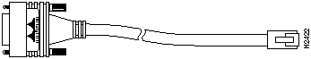
The EIA/TIA-232 console port is configured as DTE and uses an RJ-45 connector.
The router ships with a cable kit to connect a console (an ASCII terminal or PC running terminal emulation software) to the console port. The console cable kit contains an RJ-45-to-RJ-45 rollover cable and RJ-45-to-DB-9 and RJ-45-to-DB-25 female DTE adapters (labeled Terminal). Table C-1 lists pinouts for the asynchronous serial console port, the RJ-45-to-RJ-45 rollover cable, and the RJ-45-to-DB-9 and RJ-45-to-DB-25 female DTE adapters. Auxiliary port pinouts are the same as the console port pinouts.
| Auxiliary and Console Port (DTE) | RJ-45-to-RJ-45 Rollover Cable | RJ-45-to-DB-9 Adapter | RJ-45-to-DB-25 Adapter | ||
|---|---|---|---|---|---|
| Signal | RJ-45 Pin | RJ-45 Pin | DB-9 Pin | DB-25 Pin | Signal |
| RTS | 1 | 8 | 8 | 5 | CTS |
| DTR | 2 | 7 | 6 | 6 | DSR |
| TxD | 3 | 6 | 2 | 3 | RxD |
| GND | 4 | 5 | 5 | 7 | GND |
| GND | 5 | 4 | 5 | 7 | GND |
| RxD | 6 | 3 | 3 | 2 | TxD |
| DSR | 7 | 2 | 4 | 20 | DTR |
| CTS | 8 | 1 | 7 | 4 | RTS |
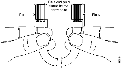
You can identify a rollover cable by comparing the modular plugs at the two ends of the cable. When you hold the plugs side by side, with the tab at the back, the wire connected to the pin on the outside of the left plug should be the same color as the wire connected to the pin on the outside of the right plug. (See Figure C-1.) If you purchased your cable from us, pin 1 is white on one connector, and pin 8 is white on the other (a rollover cable connects pins 1 and 8, 2 and 7, 3 and 6, and 4 and 5).
Figure C-1 : Identifying a Rollover Cable
All serial interface types except EIA-530 are available in DTE or DCE format: DTE with a plug connector at the network end and DCE with a receptacle at the network end. V.35 is available in either mode with either gender at the network end. EIA-530 is available in DTE only.
The tables in this section list the signal pinouts for both the DTE-mode and DCE-mode serial port adapter cables for each serial interface type.
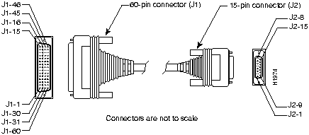
EIA/TIA-232 Serial Cable Assembly
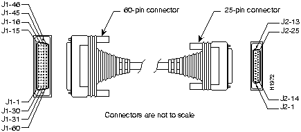
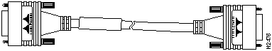
Figure C-2 shows the EIA/TIA-232 serial cable assembly; Table C-2 lists the DTE pinouts; and Table C-3 lists the DCE pinouts. Arrows indicate signal direction: ---> indicates DTE to DCE, and <--- indicates DCE to DTE.
Figure C-2 : EIA/TIA-232 Cable Assembly
| 60 Pin | Signal | Note | Direction | 25 Pin | Signal |
|---|---|---|---|---|---|
| J1-50
J1-51 J1-52 |
MODE_0
GND MODE_DCE |
Shorting group | -- | -- | -- |
| J1-46 | Shield GND | Single | -- | J2-1 | Shield GND |
| J1-46 | Shield GND | Single | -- | J2-1 | Shield GND |
| J1-41
Shield |
TXD/RXD
-- |
Twisted pair no. 5 | --->
-- |
J2-2
Shield |
TXD
-- |
| J1-36
Shield |
RXD/TXD
-- |
Twisted pair no. 9 | <---
-- |
J2-3
Shield |
RXD
-- |
| J1-42
Shield |
RTS/CTS
-- |
Twisted pair no. 4 | --->
-- |
J2-4
Shield |
RTS
-- |
| J1-35
Shield |
CTS/RTS
-- |
Twisted pair no. 10 | <---
-- |
J2-5
Shield |
CTS
-- |
| J1-34
Shield |
DSR/DTR
-- |
Twisted pair no. 11 | <---
-- |
J2-6
Shield |
DSR
-- |
| J1-45
Shield |
Circuit GND
-- |
Twisted pair no. 1 | --
-- |
J2-7
Shield |
Circuit GND
-- |
| J1-33
Shield |
DCD/LL
-- |
Twisted pair no. 12 | <---
-- |
J2-8
Shield |
DCD
-- |
| J1-37
Shield |
TXC/NIL
-- |
Twisted pair no. 8 | <---
-- |
J2-15
Shield |
TXC
-- |
| J1-38
Shield |
RXC/TXCE
-- |
Twisted pair no. 7 | <---
-- |
J2-17
Shield |
RXC
-- |
| J1-44
Shield |
LL/DCD
-- |
Twisted pair no. 2 | --->
-- |
J2-18
Shield |
LTST
-- |
| J1-43
Shield |
DTR/DSR
-- |
Twisted pair no. 3 | --->
-- |
J2-20
Shield |
DTR
-- |
| J1-39
Shield |
TXCE/TXC
-- |
Twisted pair no. 6 | --->
-- |
J2-24
Shield |
TXCE
-- |
| 60 Pin | Signal | Note | Direction | 25 Pin | Signal |
|---|---|---|---|---|---|
| J1-50
J1-51 |
MODE_0
GND |
Shorting group | --
|
--
|
--
|
| J1-36
Shield |
RXD/TXD
-- |
Twisted pair no. 9 | <---
-- |
J2-2
Shield |
TXD
-- |
| J1-41
Shield |
TXD/RXD
-- |
Twisted pair no. 5 | --->
-- |
J2-3
Shield |
RXD
-- |
| J1-35
Shield |
CTS/RTS
-- |
Twisted pair no. 10 | <---
-- |
J2-4
Shield |
RTS
-- |
| J1-42
Shield |
RTS/CTS
-- |
Twisted pair no. 4 | --->
-- |
J2-5
Shield |
CTS
-- |
| J1-43
Shield |
DTR/DSR
-- |
Twisted pair no. 3 | --->
-- |
J2-6
Shield |
DSR
-- |
| J1-45
Shield |
Circuit GND
-- |
Twisted pair no. 1 | --
-- |
J2-7
Shield |
Circuit GND |
| J1-44
Shield |
LL/DCD
-- |
Twisted pair no. 2 | --->
-- |
J2-8
Shield |
DCD
-- |
| J1-39
Shield |
TXCE/TXC
-- |
Twisted pair no. 7 | --->
-- |
J2-15
Shield |
TXC
-- |
| J1-40
Shield |
NIL/RXC
-- |
Twisted pair no. 6 | --->
-- |
J2-17
Shield |
RXC
-- |
| J1-33
Shield |
DCD/LL
-- |
Twisted pair no. 12 | <---
-- |
J2-18
Shield |
LTST
-- |
| J1-34
Shield |
DSR/DTR
-- |
Twisted pair no. 11 | <---
-- |
J2-20
Shield |
DTR
-- |
| J1-38
Shield |
RXC/TXCE
-- |
Twisted pair no. 8 | <---
-- |
J2-24
Shield |
TXCE
-- |
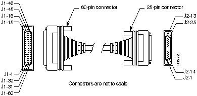
EIA/TIA-449 Serial Cable Assembly
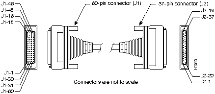
Figure C-3 shows the EIA/TIA-449 serial cable assembly; Table C-4 lists the DTE pinouts; Table C-5 lists the DCE pinouts. Arrows indicate signal direction: ---> indicates DTE to DCE, and <--- indicates DCE to DTE.
Figure C-3 : EIA/TIA-449 Serial Cable Assembly
| 60 Pin | Signal Name | Note | Direction | 37 Pin | Signal Name |
|---|---|---|---|---|---|
| J1-49
J1-48 |
MODE_1
GND |
Shorting group | -- | -- | -- |
| J1-51
J1-52 |
GND
MODE_DCE |
Shorting group | -- | -- | -- |
| J1-46 | Shield_GND | Single | _ | J2-1 | Shield GND |
| J1-11
J1-12 |
TXD/RXD+
TXD/RXD-- |
Twisted pair no. 6 | --->
---> |
J2-4
J2-22 |
SD+
SD-- |
| J1-24
J1-23 |
TXC/RXC+
TXC/RXC-- |
Twisted pair no. 9 | <---
<--- |
J2-5
J2-23 |
ST+
ST-- |
| J1-28
J1-27 |
RXD/TXD+
RXD/TXD-- |
Twisted pair no. 11 | <---
<--- |
J2-6
J2-24 |
RD+
RD-- |
| J1-9
J1-10 |
RTS/CTS+
RTS/CTS-- |
Twisted pair no. 5 | --->
---> |
J2-7
J2-25 |
RS+
RS-- |
| J1-26
J1-25 |
RXC/TXCE+
RXC/TXCE-- |
Twisted pair no. 10 | <---
<--- |
J2-8
J2-26 |
RT+
RT-- |
| J1-1
J1-2 |
CTS/RTS+
CTS/RTS-- |
Twisted pair no. 1 | <---
<--- |
J2-9
J2-27 |
CS+
CS-- |
| J1-44
J1-45 |
LL/DCD
Circuit_GND |
Twisted pair no. 12 | --->
_ |
J2-10
J2-37 |
LL
SC |
| J1-3
J1-4 |
DSR/DTR+
DSR/DTR-- |
Twisted pair no. 2 | <---
<--- |
J2-11
J2-29 |
DM+
DM-- |
| J1-7
J1-8 |
DTR/DSR+
DTR/DSR-- |
Twisted pair no. 4 | --->
---> |
J2-12
J2-30 |
TR+
TR-- |
| J1-5
J1-6 |
DCD/DCD+
DCD/DCD-- |
Twisted pair no. 3 | <---
<--- |
J2-13
J2-31 |
RR+
RR-- |
| J1-13
J1-14 |
TXCE/TXC+
TXCE/TXC-- |
Twisted pair no. 7 | --->
---> |
J2-17
J2-35 |
TT+
TT-- |
| J1-15
J1-16 |
Circuit_GND
Circuit_GND |
Twisted pair no. 9 | --
-- |
J2-19
J2-20 |
SG
RC |
| 60 Pin | Signal Name | Note | Direction | 37 Pin | Signal Name |
|---|---|---|---|---|---|
| J1-49
J1-48 |
MODE_1
GND |
Shorting group | -- | -- | -- |
| J1-46 | Shield_GND | Single | -- | J2-1 | Shield GND |
| J1-28
J1-27 |
RXD/TXD+
RXD/TXD-- |
Twisted pair no. 11 | <---
<--- |
J2-4
J2-22 |
SD+
SD-- |
| J1-13
J1-14 |
TXCE/TXC+
TXCE/TXC-- |
Twisted pair no. 7 | --->
---> |
J2-5
J2-23 |
ST+
ST-- |
| J1-11
J1-12 |
TXD/RXD+
TXD/RXD-- |
Twisted pair no. 6 | --->
---> |
J2-6
J2-24 |
RD+
RD-- |
| J1-1
J1-2 |
CTS/RTS+
CTS/RTS-- |
Twisted pair no. 1 | <---
<--- |
J2-7
J2-25 |
RS+
RS-- |
| J1-24
J1-23 |
TXC/RXC+
TXC/RXC-- |
Twisted pair no. 9 | --->
---> |
J2-8
J2-26 |
RT+
RT-- |
| J1-9
J1-10 |
RTS/CTS+
RTS/CTS-- |
Twisted pair no. 5 | --->
---> |
J2-9
J2-27 |
CS+
CS-- |
| J1-29
J1-30 |
NIL/LL
Circuit_GND |
Twisted pair no. 12 | --->
-- |
J2-10
J2-37 |
LL
SC |
| J1-7
J1-8 |
DTR/DSR+
DTR/DSR-- |
Twisted pair no. 4 | --->
---> |
J2-11
J2-29 |
DM+
DM-- |
| J1-3
J1-4 |
DSR/DTR+
DSR/DTR-- |
Twisted pair no. 2 | <---
<--- |
J2-12
J2-30 |
TR+
TR-- |
| J1-5
J1-6 |
DCD/DCD+
DCD/DCD-- |
Twisted pair no. 3 | --->
---> |
J2-13
J2-31 |
RR+
RR-- |
| J1-26
J1-25 |
RXC/TXCE+
RXC/TXCE-- |
Twisted pair no. 10 | <---
<--- |
J2-17
J2-35 |
TT+
TT-- |
| J1-15
J1-16 |
Circuit_GND
Circuit_GND |
Twisted pair no. 8 | _
_ |
J2-19
J2-20 |
SG
RC |
Figure C-4 shows the V.35 serial cable assembly; Table C-6 lists the DTE pinouts; Table C-7 lists the DCE pinouts. Arrows indicate signal direction: ---> indicates DTE to DCE, and <--- indicates DCE to DTE.
Figure C-4 : V.35 Serial Cable Assembly
| 60 Pin | Signal Name | Type | Direction | 34 Pin | Signal Name |
|---|---|---|---|---|---|
| J1-49
J1-48 |
MODE_1
GND |
Shorting group | -- | -- | -- |
| J1-50
J1-51 J1-52 |
MODE_0
GND MODE_DCE |
Shorting group | -- | -- | -- |
| J1-53
J1-54 J1-55 J1-56 |
TxC/NIL
RxC_TxCE RxD/TxD GND |
Shorting group | -- | -- | -- |
| J1-46 | Shield_GND | Single | -- | J2-A | Frame GND |
| J1-45
Shield |
Circuit_GND
-- |
Twisted pair no. 12 | --
-- |
J2-B
Shield |
Circuit GND
-- |
| J1-42
Shield |
RTS/CTS
-- |
Twisted pair no. 9 | --->
-- |
J2-C
Shield |
RTS
-- |
| J1-35
Shield |
CTS/RTS
-- |
Twisted pair no. 8 | <---
-- |
J2-D
Shield |
CTS
-- |
| J1-34
Shield |
DSR/DTR
-- |
Twisted pair no. 7 | <---
-- |
J2-E
Shield |
DSR
-- |
| J1-33
Shield |
DCD/LL
-- |
Twisted pair no. 6 | <---
-- |
J2-F
Shield |
RLSD
-- |
| J1-43
Shield |
DTR/DSR
-- |
Twisted pair no. 10 | --->
-- |
J2-H
Shield |
DTR
-- |
| J1-44
Shield |
LL/DCD
-- |
Twisted pair no. 11 | --->
-- |
J2-K
Shield |
LT
-- |
| J1-18
J1-17 |
TxD/RxD+
TxD/RxD-- |
Twisted pair no. 1 | --->
---> |
J2-P
J2-S |
SD+
SD-- |
| J1-28
J1-27 |
RxD/TxD+
RxD/TxD-- |
Twisted pair no. 5 | <---
<--- |
J2-R
J2-T |
RD+
RD-- |
| J1-20
J1-19 |
TxCE/TxC+
TxCE/TxC-- |
Twisted pair no. 2 | --->
---> |
J2-U
J2-W |
SCTE+
SCTE-- |
| J1-26
J1-25 |
RxC/TxCE+
RxC/TxCE-- |
Twisted pair no. 4 | <---
<--- |
J2-V
J2-X |
SCR+
SCR-- |
| J1-24
J1-23 |
TxC/RxC+
TxC/RxC-- |
Twisted pair no. 3 | <---
<--- |
J2-Y
J2-AA |
SCT+
SCT-- |
| 60 Pin | Signal Name | Type | Direction | 34 Pin | Signal Name |
|---|---|---|---|---|---|
| J1-49
J1-48 |
MODE_1
GND |
Shorting group | -- | -- | -- |
| J1-50
J1-51 |
MODE_0
GND |
Shorting group | -- | -- | -- |
| J1-53
J1-54 J1-55 J1-56 |
TxC/NIL
RxC_TxCE RxD/TxD GND |
Shorting group | -- | -- | -- |
| J1-46 | Shield_GND | Single | -- | J2-A | Frame GND |
| J1-45
Shield |
Circuit_GND
-- |
Twisted pair no. 12 | --
-- |
J2-B
Shield |
Circuit GND
-- |
| J1-35
Shield |
CTS/RTS
-- |
Twisted pair no. 8 | <---
-- |
J2-C
Shield |
RTS
-- |
| J1-42
Shield |
RTS/CTS
-- |
Twisted pair no. 9 | --->
-- |
J2-D
Shield |
CTS
-- |
| J1-43
Shield |
DTR/DSR
-- |
Twisted pair no. 10 | --->
-- |
J2-E
Shield |
DSR
-- |
| J1-44
Shield |
LL/DCD
-- |
Twisted pair no. 11 | --->
-- |
J2-F
Shield |
RLSD
-- |
| J1-34
Shield |
DSR/DTR
-- |
Twisted pair no. 7 | <---
-- |
J2-H
Shield |
DTR
-- |
| J1-33
Shield |
DCD/LL
-- |
Twisted pair no. 6 | <---
-- |
J2-K
Shield |
LT
-- |
| J1-28
J1-27 |
RxD/TxD+
RxD/TxD-- |
Twisted pair no. 5 | <---
<--- |
J2-P
J2-S |
SD+
SD-- |
| J1-18
J1-17 |
TxD/RxD+
TxD/RxD-- |
Twisted pair no. 1 | --->
---> |
J2-R
J2-T |
RD+
RD-- |
| J1-26
J1-25 |
RxC/TxCE+
RxC/TxCE-- |
Twisted pair no. 4 | <---
<--- |
J2-U
J2-W |
SCTE+
SCTE-- |
| J1-22
J1-21 |
NIL/RxC+
NIL/RxC-- |
Twisted pair no. 3 | --->
---> |
J2-V
J2-X |
SCR+
SCR-- |
| J1-20
J1-19 |
TxCE/TxC+
TxCE/TxC-- |
Twisted pair no. 2 | --->
---> |
J2-Y
J2-AA |
SCT+
SCT-- |
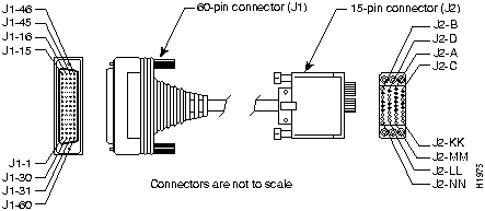
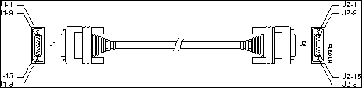
Figure C-5 shows the X.21 serial cable assembly; Table C-8 lists the DTE pinouts; Table C-9 lists the DCE pinouts. Arrows indicate signal direction: ---> indicates DTE to DCE, and <--- indicates DCE to DTE.
Figure C-5 : X.21 Serial Cable Assembly
| 60 Pin | Signal Name | Type | Direction | 15 Pin | Signal Name |
|---|---|---|---|---|---|
| J1-48
J1-47 |
GND
MODE_2 |
Shorting group | - | -- | -- |
| J1-51
J1-52 |
GND
MODE_DCE |
Shorting group | -- | -- | -- |
| J1-46 | Shield_GND | Single | -- | J2-1 | Shield GND |
| J1-11
J1-12 |
TXD/RXD+
TXD/RXD-- |
Twisted pair no. 3 | --->
---> |
J2-2
J2-9 |
Transmit+
Transmit-- |
| J1-9
J1-10 |
RTS/CTS+
RTS/CTS-- |
Twisted pair no. 2 | --->
---> |
J2-3
J2-10 |
Control+
Control-- |
| J1-28
J1-27 |
RXD/TXD+
RXD/TXD-- |
Twisted pair no. 6 | <---
<--- |
J2-4
J2-11 |
Receive+
Receive-- |
| J1-1
J1-2 |
CTS/RTS+
CTS/RTS-- |
Twisted pair no. 1 | <---
<--- |
J2-5
J2-12 |
Indication+
Indication-- |
| J1-26
J1-25 |
RXC/TXCE+
RXC/TXCE-- |
Twisted pair no. 5 | <---
<--- |
J2-6
J2-13 |
Timing+
Timing-- |
| J1-15
Shield |
Control_GND
-- |
Twisted pair no. 4 | --
-- |
J2-8
Shield |
Control GND
-- |
| 60 Pin | Signal Name | Type | Direction | 15 Pin | Signal Name |
|---|---|---|---|---|---|
| J1-48
J1-47 |
GND
MODE_2 |
Shorting group | -- | -- | -- |
| J1-46 | Shield_GND | Single | -- | J2-1 | Shield GND |
| J1-28
J1-27 |
RXD/TXD+
RXD/TXD-- |
Twisted pair no. 6 | <---
<--- |
J2-2
J2-9 |
Transmit+
Transmit-- |
| J1-1
J1-2 |
CTS/RTS+
CTS/RTS-- |
Twisted pair no. 1 | <---
<--- |
J2-3
J2-10 |
Control+
Control-- |
| J1-11
J1-12 |
TXD/RXD+
TXD/RXD-- |
Twisted pair no. 3 | --->
---> |
J2-4
J2-11 |
Receive+
Receive-- |
| J1-9
J1-10 |
RTS/CTS+
RTS/CTS-- |
Twisted pair no. 2 | --->
---> |
J2-5
J2-12 |
Indication+
Indication-- |
| J1-24
J1-23 |
TXC/RXC+
TXC/RXC-- |
Twisted pair no. 4 | --->
---> |
J2-6
J2-13 |
Timing+
Timing-- |
| J1-15
Shield |
Control_GND
-- |
Twisted pair no. 5 | --
-- |
J2-8
Shield |
Control GND
-- |
Figure C-6 shows the EIA-530 serial cable assembly, and Table C-10 lists the pinouts. Arrows indicate signal direction: ---> indicates DTE to DCE, and <--- indicates DCE to DTE.
Figure C-6 : EIA-530 Serial Cable Assembly
|
60 Pin |
Signal Name |
25 Pin |
Signal Name |
Direction
DTE DCE1 |
|---|---|---|---|---|
| J1-11
J1-12 |
TXD/RXD+
TXD/RXD-- |
J2-2
J2-14 |
BA(A), TXD+
BA(B), TXD-- |
--->
---> |
| J1-28
J1-27 |
RXD/TXD+
RXD/TXD-- |
J2-3
J2-16 |
BB(A), RXD+
BB(B), RXD-- |
<---
<--- |
| J1-9
J1-10 |
RTS/CTS+
RTS/CTS-- |
J2-4
J2-19 |
CA(A), RTS+
CA(B), RTS-- |
--->
---> |
| J1-1
J1-2 |
CTS/RTS+
CTS/RTS-- |
J2-5
J2-13 |
CB(A), CTS+
CB(B), CTS-- |
<---
<--- |
| J1-3
J1-4 |
DSR/DTR+
DSR/DTR-- |
J2-6
J2-22 |
CC(A), DSR+
CC(B), DSR-- |
<---
<--- |
| J1-46
J1-47 |
Shield_GND
MODE_2 |
J2-1
-- |
Shield
-- |
Shorted |
| J1-48
J1-49 |
GND
MODE_1 |
--
-- |
--
-- |
Shorted |
| J1-5
J1-6 |
DCD/DCD+
DCD/DCD-- |
J2-8
J2-10 |
CF(A), DCD+
CF(B), DCD-- |
<---
<--- |
| J1-24
J1-23 |
TXC/RXC+
TXC/RXC-- |
J2-15
J2-12 |
DB(A), TXC+
DB(B), TXC-- |
<---
<--- |
| J1-26
J1-25 |
RXC/TXCE+
RXC/TXCE-- |
J2-17
J2-9 |
DD(A), RXC+
DD(B), RXC-- |
<---
<--- |
| J1-44
J1-45 |
LL/DCD
Circuit_GND |
J2-18
J2-7 |
LL
Circuit_ GND |
--->
-- |
| J1-7
J1-8 |
DTR/DSR+
DTR/DSR-- |
J2-20
J2-23 |
CD(A), DTR+
CD(B), DTR-- |
--->
---> |
| J1-13
J1-14 |
TXCE/TXC+
TXCE/TXC-- |
J2-24
J2-11 |
DA(A), TXCE+
DA(B), TXCE-- |
--->
---> |
| J1-51
J1-52 |
GND
MODE_DCE |
--
-- |
--
-- |
Shorted |
This section provides the pinouts and signal descriptions for the Ethernet (AUI) cable and 10BaseT connector.
Figure C-7 shows the Ethernet (AUI) cable assembly and Table C-11 lists the pinouts.
Figure C-7 : Ethernet (AUI) Cable Assembly
| Pin | Ethernet Circuit | Signal Name |
|---|---|---|
| 3 | DO-A | Data Out Circuit A |
| 10 | DO-B | Data Out Circuit B |
| 11 | DO-S | Data Out Circuit Shield |
| 5 | DI-A | Data In Circuit A |
| 12 | DI-B | Data In Circuit B |
| 4 | DI-S | Data In Circuit Shield |
| 7 | CO-A | Control Out Circuit A (not connected) |
| 15 | CO-B | Control Out Circuit B (not connected) |
| 8 | CO-S | Control Out Circuit Shield (not connected) |
| 2 | CI-A | Control In Circuit A |
| 9 | CI-B | Control In Circuit B |
| 1 | CI-S | Control In Circuit Shield |
| 6 | VC | Voltage Common |
| 13 | VP | Voltage Plus |
| 14 | VS | Voltage Shield (L25 and M25) |
| Shell | PG | Protective Ground |
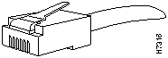
Figure C-8 shows the 10BaseT (RJ-45) connector, and Table C-12 lists the pinouts.
Figure C-8 : 10BaseT RJ-45 Connector
| Pin | Description |
|---|---|
| 1 | TX+ |
| 2 | TX-- |
| 3 | RX+ |
| 4 | -- |
| 5 | -- |
| 6 | RX-- |
| 7 | -- |
| 8 | -- |
The 1E1R 2-slot module provides both UTP and STP Token Ring connections.
Table C-13 shows the Token Ring STP port pinouts used by the 1E1R 2-slot module.
| 9-Pin | Signal Name |
|---|---|
| 1 | RX-- |
| 2 | Ground |
| 3 | +5 Volt, fused |
| 4 | Ground |
| 5 | TX-- |
| 6 | +RX |
| 7 | Ground |
| 8 | Ground |
| 9 | +TX |
Table C-14 shows the Token Ring UTP port pinouts used by the 1E1R 2-Slot module.
| RJ-45 Pins | Signal |
|---|---|
| 1 | GND |
| 2 | GND |
| 3 | Tx |
| 4 | Rx |
| 5 | Tx |
| 6 | Rx |
| 7 | GND |
| 8 | Not used |
The BRI port pinouts are shown in Table C-15.
Table C-15 : BRI Port (RJ-45) Pinouts
| 8 Pin1 | TE2 | NT3 | Polarity |
|---|---|---|---|
| 3 | Transmit | Receive | + |
| 4 | Receive | Transmit | + |
| 5 | Receive | Transmit | -- |
| 6 | Transmit | Receive | -- |
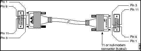
Two standard T1 serial cables are available for the CT1/PRI module: null-modem and straight-through. A straight-through cable connects the router to an external CSU. Null-modem cables are used for back-to-back operation and testing.
The T1 interface cable has two 15-pin DB connectors at each end to connect the CT1/PRI with the external T1 CSU. Figure C-9 shows the T1 interface cable, connectors, and pinouts. Table C-16 lists the pinouts for the null-modem T1 cable and Table C-17 lists the pinouts for the straight-through T1 cable.
Figure C-9 : T1 Interface Cable
Table C-16 : Null-Modem T1 Cable Pinouts
Table C-17 : Straight-Through T1 Cable Pinouts
Table C-18 lists the CT1/PRI-CSU module port pinouts. Use a straight-through RJ-48C-to-RJ-48C cable to connect the T1 port to an RJ-48C jack.
Table C-18 : CT1/PRI-CSU module Port (RJ-48C) Pinouts
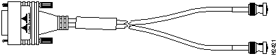
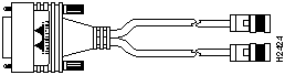
Cisco Systems makes four cables for the CE1/PRI module s. All four have DB-15 connectors on the CE1/PRI end and either BNC, DB-15, Twinax, or RJ-45 connectors on the network end. Figure C-10, to Figure C-13 show the CE1/PRI interface cables.
Figure C-10 : E1 Interface Cable for 75-Ohm, Unbalanced Connections with BNC Connectors
Figure C-11 : E1 Interface Cable for 120-Ohm, Balanced Connections with DB-15 Connectors
Figure C-12 : E1 Interface Cable for 120-Ohm, Balanced Connections with Twinax Connectors
Figure C-13 : E1 Interface Cable for 120-Ohm, Balanced Connections with an RJ-45 Connector
Table C-19 lists the Pinouts for the CE1/PRI interface cables.
Table C-19 : E1 Interface Cable Pinouts
Copyright 1988-1996 © Cisco Systems Inc.
![]()
15-Pin DB Connector
15-Pin DB Connector
Signal
Pin
Pin
Signal
Transmit Tip
1
3
Receive Tip
Receive Tip
3
1
Transmit Tip
Transmit Ring
9
11
Receive Ring
Receive Ring
11
9
Transmit Ring
15-Pin DB Connector
15-Pin DB Connector
Signal
Pin
Pin
Signal
Transmit Tip
1
1
Transmit Tip
Transmit Ring
9
9
Transmit Ring
Receive Tip
3
3
Receive Tip
Receive Ring
11
11
Receive Ring
RJ-48C Pin
Description
1
Receive Ring
2
Receive Tip
4
Ring
5
Tip
CE1/PRI End
Network End
DB-15
BNC
DB-15
Twinax
RJ-45
Pin
Signal1
Signal
Pin
Signal
Pin
Signal
Pin
Signal
9
TX Tip
TX Tip
1
TX Tip
TX-1
TX Tip
1
TX Tip
2
TX Ring
TX Shield
9
TX Ring
TX-2
TX Ring
2
TX Ring
10
TX Shield
--
2
TX Shield
Shield
TX Shield
3
TX Shield
8
RX Tip
RX Tip
3
RX Tip
RX-1
RX Tip
4
RX Tip
15
RX Ring
RX Shield
11
RX Ring
RX-2
RX Ring
5
RX Ring
7
RX Shield
--
4
RX Shield
Shield
RX Shield
6
RX Shield
1 TX = transmit. RX = receive.
![]()
![]()
![]()
![]()
![]()
![]()
![]()
![]()