|
|
This appendix presents memory maps for selected product platforms, processors, and interface cards. Memory map information is useful for technically qualified users who understand concepts of low-level operating systems and have a basic understanding of bus structures and address mapping in computer systems.
When using this appendix, be aware of the distinct difference between program counter values and operand addresses. The addresses that appear in this appendix are operand values and should not be confused with program counter values.
Memory Maps and Troubleshooting
Memory map information can be useful when you are determining whether a problem exists in the software or in the hardware. The system software can provide information on the reasons for a system crash. This information appears in the form of error messages issued by the read-only memory (ROM) monitor when an exception is encountered.
When a system crashes, the ROM monitor reports a failure type. The failure type is important both in its own right and as a guide to interpreting the other information the system provides. Failure types are usually one of the following:
The system encounters a bus error when the processor tries to use a device or a memory location that either does not exist or does not respond properly. Bus errors indicate either a software bug or a hardware problem. The address the processor was trying to access when the system crashed provides a key as to whether the failure is due to software or hardware.
If the operand address is valid, the problem is probably in the hardware. The address maps list addresses for selected hardware platforms.
Bus errors on an address not in the map usually indicate a software bug.
Address errors occur when the software tries to access data on incorrectly aligned boundaries. For example, 2- and 4-byte accesses are allowed only on even addresses. An address error usually indicates a software bug.
Cisco processors have timers that guard against certain types of system hangs. The central processing unit (CPU) periodically resets a watchdog timer. If the timer is not reset, a trap will occur. Failure to service the watchdog timer indicates either a hardware or a software bug.
Parity errors indicate that internal hardware error checks have failed. A parity failure is almost certainly a hardware problem. Use the address map to locate the affected hardware.
Emulator traps indicate that the processor has executed an illegal instruction. Emulator traps can be caused either by software taking illegal branches or by hardware failures, notably ROM failures.
By observing the operand address, you can locate the general area of the router where the error occurred. Hardware problems can be inferred only from a bus error on a legal address, not from an emulator trap or illegal instruction trap. When looking at the bus error, the operand address---not the program counter address---provides the memory map location of the error.
By using the show stacks EXEC command, you can display data saved by the ROM monitor, which includes a failure type, an operand address, and a failure program counter. This data is overwritten when the system is reloaded, so you might want to check your configuration register settings and decide how you want to recover from system crashes. Stack traces can be used by qualified technical support representatives who have access to symbol tables, object files, and source code.
Figure D-1 shows an example of the show stacks output from a software failure. The message "Software forced crash" indicates that the software detected a condition it did not expect and from which it could not recover. When investigated by a technical support representative, the listed program counter provides a trace to the code responsible for the failure.
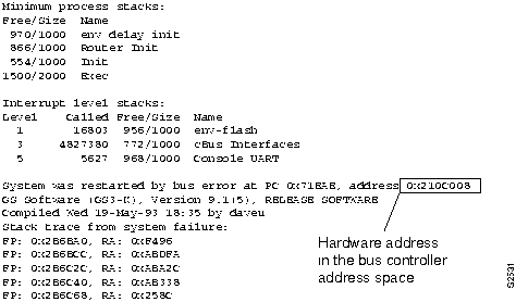
Figure D-2 shows output from a hardware error and includes an example of a hardware operand address that can be used with the memory maps in this appendix. The operand address points to the register space for MCI unit 0 and indicates a hardware or microcode problem with that unit.
Figure D-1 : show stacks Command Output Showing the Software Program Counter Address
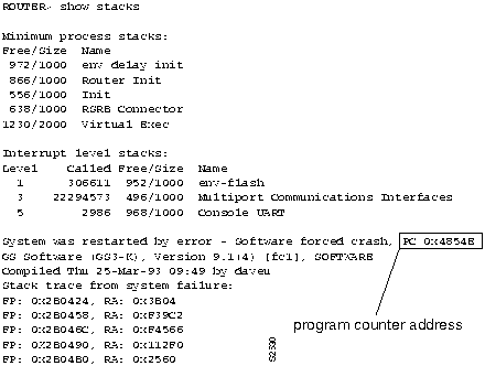
Figure D-2 : show stacks Command Output Showing the Hardware Address
The following tables summarize memory map information for the various Cisco platforms:
Table D-1 : Cisco 2000 Memory Map
| Address | Description | Comments |
|---|---|---|
| 00000000 - 0017FFFF | CPU and packet memory (dynamic random-access memory [DRAM]) | 1.5 MB |
| 01000000 - 011FFFFF | ROM monitor and system image code space (erasable programmable read-only memory [EPROM]) | 2 MB |
| 02000000 - 02007FFF | Configuration random-access memory (RAM) | 32 KB |
| 02100000 - 0213FFFF | Control registers and input/output (I/O) devices | Details follow |
| 02110000 | Control register 1 | -- |
| 02110002 | Control register 2 | -- |
| 02110040 | Programmable read-only memory (PROM) cookie | -- |
| 02110100 | Status register | -- |
| 02120040 | Timer control register | -- |
| 02130000 - 02130003 | Ethernet controller | -- |
| 02130000 - 0213000F | Token Ring controller | -- |
| 02130040 - 02130043 | Serial controller | -- |
| 02130080 | Serial control register 1 | -- |
| 02130081 | Serial control register 2 | -- |
Table D-2 : Cisco 2500 Memory Map
| Address | Bit Width | Description | Comments |
|---|---|---|---|
| 00000000 - 00FFFFFF | 32 | DRAM | 2, 4, 8, or 16 MB |
| 00000000 - 001FFFFF | 32 | DRAM 2 MB | -- |
| 00000000 - 003FFFFF | 32 | DRAM 4 MB | -- |
| 00000000 - 007FFFFF | 32 | DRAM 8 MB | -- |
| 00000000 - 00FFFFFF | 32 | DRAM 16 MB | -- |
| 00000000 - 001FFFFF | 8/16 | Boot Flash memory | 1 or 2 MB, when Flash memory PCMCIA card is not installed |
| 00000000 - 001FFFFF | 16 | Flash memory PCMCIA card | Boot Mode |
| 01000000 - 011FFFFF | 16 | Boot EPROMs for ROM monitor and RXBOOT images | 1 or 2 MB ROM; 2 MB Flash memory |
| 01000000 - 011FFFFF | 16 | Flash memory PCMCIA card | When installed |
| 02000000 - 0201FFFF | 8 | Configuration non-volatile random-access memory (NVRAM) | 32 or 128 KB |
| 02000000 - 02007FFF | 8 | Configuration NVRAM (32 KB) | -- |
| 02000000 - 0201FFFF | 8 | Configuration NVRAM (128 KB) | -- |
| 02100000 - 0213FFFF | 8/16 | Onboard I/O registers and chips | -- |
| 03000000 - 03FFFFFF | 32 | Flash memory RAM (SIMMs) | 4, 8, or 16 MB |
| 03000000 - 033FFFFF | 32 | Flash memory RAM (4 MB) | -- |
| 03000000 - 037FFFFF | 32 | Flash memory RAM (8 MB) | -- |
| 03000000 - 03FFFFFF | 32 | Flash memory RAM (16 MB) | -- |
| 08000000 - 081FFFFF | 8/16 | Onboard boot EPROMs (remapped) | 1 or 2 MB, when PCMCIA Flash memory card is installed |
Table D-3 : Cisco 3000 Memory Map
| Address | Description | Comments |
|---|---|---|
| 00000000 - 00FFFFFF | Main memory DRAM | -- |
| 01000000 - 011FFFFF | Secondary DRAM | -- |
| 02000000 - 0201FFFF | NVRAM | -- |
| 02100000 - 02100FFF | Channel B: 68302 registers | -- |
| 02101000 - 02101FFF | Channel B: 63802 RAM | -- |
| 02110000 | System control register 1 | -- |
| 02110002 | System control register 2 | -- |
| 02110100 | System status register | -- |
| 02110040 - 0211005F | Cookie | -- |
| 02120000 - 02120003 | Counter/timer (CNTR) | -- |
| 02120040 | Counter control register (CCTL) | -- |
| 02120100 - 0212013F | Console ports | -- |
| 02130000 - 02130003 | Channel A: LANCE chip | -- |
| 02130040 - 02130043 | Channel B: LANCE/serial chip | -- |
| 02130080 - 02130083 | Channel B: serial DTR register | -- |
| 03000000 - 03FFFFFF | Flash memory | -- |
| 04000000 - 042FFFFF | Secondary RAM | When main memory = 16 MB |
Table D-4 : Cisco 3104 and Cisco 3204 Memory Map
| Address | Description | Comments |
|---|---|---|
| 00000000 - 00FFFFFF | Main DRAM | 1-, 4-, 8-, and 16-MB sizes |
| 01000000 - 010FFFFF | Boot EPROMs for ROM monitor and bootstrap image | -- |
| 01000000 - 011FFFFF | Boot Flash memory for ROM monitor and bootstrap image | Onboard Flash memory or PCMCIA Flash memory card, 2 MB |
| 02000000 - 0201FFFF | Configuration NVRAM | 32 or 128 KB size |
| 02100000 - 0213FFFF | Onboard registers and chips | -- |
| 03000000 - 03FFFFFF | Flash memory single in-line memory module (SIMM) | Up to 16 MB |
| 04000000 - 041FFFFF | I/O memory (packet memory) | 512 KB or 2 MB sizes |
| 08000000 - 081FFFFF | Remapped onboard boot Flash memory | Remapped when PCMCIA Flash memory card is installed |
Table D-5 : Cisco 3104 and Cisco 3204 Onboard Registers and Chips
| Address | Description | Comments |
|---|---|---|
| 021000F2 - 021000F3 | Base address register for 68302 | -- |
| 021000F4 - 021000F7 | System control register for 68302 | -- |
| 02101000 - 021013FF | System RAM for 68302 | -- |
| 02101400 - 021017FF | Parameter RAM for 68302 | -- |
| 02101800 - 02101FFF | Internal registers for 68302 | -- |
| 02110000 | System control register 1 | -- |
| 02110002 | System control register 2 | -- |
| 02110004 | System control register 3 | -- |
| 02110006 | System interrupt register | -- |
| 02110060 | Serial NVRAM control register | -- |
| 02120000 - 02120003 | Timer counter | -- |
| 02120040 | Counter control register | -- |
| 02120100 - 0212013F | Console interfaces | -- |
| 02130000 - 0213003 | Ethernet controller | -- |
| 02131000 - 0213100F | Token Ring controller | -- |
| 02131010 - 02131011 | Hardware map register 0 | -- |
| 02131012 - 02131013 | Hardware map register 1 | -- |
| 02132000 - 021320FF | Serial controller | -- |
| 02132100 - 02132101 | Serial 0 device register | -- |
| 02132102 - 02132103 | Serial 1 device register | -- |
Table D-6 : Cisco 4000 Memory Map
| Address | Bit Width | Description | Comments |
|---|---|---|---|
| 00000000 - 0003FFFF | 32 | System static random-access memory (SRAM) | 256 KB, fixed; 0 wait read, 1 wait write |
| 00040000 - 00FFFFFF | 32 | System DRAM memory (SIMMs) | 8-, 16-, 32-bit unaligned access supported; 4, 8, 16, or 321 MB |
| 00040000 - 003FFFFF | 4 MB | -- | |
| 00040000 - 00FFFFFF | 16 MB | -- | |
| 01000000 - 01FFFFFF | 16 | Boot EPROM | 2 MB, fixed |
| 01000000 - 010FFFFF | 1 MB | -- | |
| 01000000 - 011FFFFF | 2 MB | -- | |
| 01000000 - 013FFFFF | 4 MB | -- | |
| 01000000 - 017FFFFF | 8 MB | -- | |
| 02000000 - 02FFFFFF | 8 or 32 | Onboard resources | -- |
| 02020000 | System I/O | -- | |
| 03000000 - 03FFFFFF | 32 | Flash memory EPROM or EPROM | 32 bit read/write access |
| 03000000 - 031FFFFF | 2 MB | -- | |
| 03000000 - 033FFFFF | 4 MB | -- | |
| 03000000 - 037FFFFF | 8 MB2 | -- | |
| 05000000 | System DRAM | Upper 16 MB of 32 MB configuration | |
| 06000000 - 06FFFFFF | 32 | Shared (I/O) memory | 8-, 16-, 32-bit unaligned access supported; 1--16 MB |
| 06000000 - 060FFFFF | 1 MB | -- | |
| 06000000 - 063FFFFF | 4 MB | -- | |
| 06000000 - 067FFFFF | 8 MB | -- | |
| 04000000 - 05FFFFFF | Undefined | -- | |
| 07000000 - 07FFFFFF | Undefined | -- | |
| 08000000 - 08FFFFFF | 32 | I/O expansion | Network interface module (NIM) slots |
| 08000000 - 080FFFFF | 16 | NIM at I/O expansion slot 1 | 16 bit aligned access only |
| 08100000 - 081FFFFF | 16 | NIM at I/O expansion slot 2 | 16 bit aligned access only |
| 08200000 - 082FFFFF | 16 | NIM at I/O expansion slot 3 | 16 bit aligned access only |
Table D-7 : Cisco 4000 Memory Map of Onboard Resources
| Address | Bit Width | Description | Comments |
|---|---|---|---|
| 02000000 - 0201FFFF | 8 | NVRAM battery backed up CMOS SRAM | 128 KB, fixed; also accommodates 32 KB x 8 and 8 KB x 8 |
| 02110000 | 32 | System status and control registers | -- |
| 02110002 | Hardware revision | -- | |
| 02110040 - 0211005F | 8 | System ID PROM cookie | 24 bytes |
| 02110100 | 32 | Shared memory control register | -- |
| 02120000 | 8 | Counter timer | -- |
| 02120040 | 8 | Counter interrupt control register | -- |
| 02120100 - 0212013F | 8 | Control serial I/O | -- |
Table D-8 : Cisco 4500 Memory Map
| Address | Bit Width | Description | Comments |
|---|---|---|---|
| 60000000 - 61FFFFFF | 64 | System DRAM | Capable of 8--64 bit access, cached |
| 60000000 - 607FFFFF | 8 MB | -- | |
| 60000000 - 60FFFFFF | 16 MB | -- | |
| 60000000 - 61FFFFFF | 32 MB | -- | |
| BFC00000 - BFC7FFFF | 8 | Boot EPROM | -- |
| BFC00000 - BFC1FFFF | 128 KB | -- | |
| BFC00000 - BFC7FFFF | 512 KB | -- | |
| 3E000000 - 3EFFFFFF | 8 | Onboard resources | -- |
| 30000000 - 30FFFFFF | 32 | System Flash memory EPROM | -- |
| 30000000 - 303FFFFF | 4 MB | -- | |
| 30000000 - 307FFFFF | 8 MB | -- | |
| 30000000 - 30FFFFFF | 16 MB | -- | |
| 38000000 - 387FFFFF | 32 | Boot Flash memory EPROM | -- |
| 38000000 - 383FFFFF | 4 MB | -- | |
| 38000000 - 387FFFFF | 8 MB | -- | |
| 40000000 - 40FFFFFF | 32 | Shared memory | 8-, 16-, 32-bit access |
| 40000000 - 403FFFFF | 4 MB | -- | |
| 40000000 - 40FFFFFF | 16 MB | -- |
Table D-9 : Cisco 4500 Memory Map of Onboard Resources
| Address | Bit Width | Description | Comments |
|---|---|---|---|
| 3E000000 - 3E07FFFF | 8 | NVRAM | Battery backed up SRAM |
| 3E000000 - 3E01FFFF | 8 | 128 KB | -- |
| 3E000000 - 3E07FFFF | 8 | 512 KB | -- |
| 3E000000 | 8 | Time of day clock | -- |
| 3E800400 | 8 | System ID PROM cookie | -- |
Table D-10 : Cisco 7000 Memory Map
| Address | Description | Comments |
|---|---|---|
| 11110100 | System status register | -- |
| 11110400 | Flash memory card status | -- |
| 11110C00 | I/O address base | SwitchBus address space. Each unit occupies 64 bytes (0x40). |
| 11120040 | Timer control register | -- |
| 11120200 | Environmental monitor control | 16 bits |
| 11120300 | Environmental monitor status | 32 bits |
| 11130000 | Diagnostic bus | -- |
| 11131000 | ID PROM | -- |
| 11140000 | NVRAM | -- |
| 1115FC00 | Environmental monitor NVRAM base address | -- |
| 1115FFFF | Real time calendar bit | -- |
| 11200000 - 11FFFFFF | Reserved | 14 Mb reserved |
| 12000000 | Onboard Flash memory | -- |
| 14000000 | External Flash memory | -- |
Table D-11 : Cisco 500-CS Memory Map
| Address | Description | Comments |
|---|---|---|
| 000000 - 3FFFFF | ROM | 4 MB or less |
| 400000 - 407FFF | Electronically erasable programmable read-only memory (EEPROM) (NVRAM) | 32 KB |
| 420000 - 427FFF | LCD registers (not used) | -- |
| 428000 - 42FFFF | Future hardware | -- |
| 430000 - 440000 | Reserved | -- |
| 460000 - 460004 | LANCE registers | Ethernet controller registers |
| 500000 - 50007F | Octal Universal Asynchronous Receiver/Transmitter (UART) 0 | -- |
| 500400 - 50047F | Octal UART 1 | -- |
| 600000 - 7FFFFF | Onboard RAM | -- |
| 800000 - BFFFFF | 2-MB SIMM expansion | -- |
| 800000 - FFFFFF | 8-MB SIMM expansion | -- |
Table D-12 : Multibus Memory Space Assignment
| Address | Description | Comments |
|---|---|---|
| 20000000 - 2000FFFF | Memory card | 64 KB |
| 20010000 - 2002FFFF | CSC-R16 card | Unit 0 address, 128 KB |
| 20030000 - 2004FFFF | CSC-R16 card | Unit 1 address, 128 KB |
| 20050000 - 2006FFFF | CSC-R16 card | Unit 2 address, 128 KB |
| 20070000 - 2008FFFF | CSC-R16 card | Unit 3 address, 128 KB |
| 20090000 - 200AFFFF | CSC-R16 card | Unit 4 address, 128 KB |
| 200B0000 - 200BFFFF | NVRAM | 64 KB |
| 200C0000 - 200DFFFF | CSC-R16 card | Unit 5 address, 128 KB |
| 200E0000 - 200FFFFF | CSC-R16 card | Unit 6 address, 128 KB (shared) |
Table D-13 : Multibus I/O Space Assignment
| Address | Description | Size (in hex) | Comments |
|---|---|---|---|
| 20100000 | Environmental Monitor (ENVM) card | 2 | Environmental monitor |
| 20100002 - 2010008F | Unused | ||
| 20100090 | 2 | CSC-R16M Ethernet mailbox, Unit 0 | |
| 20100092 | 2 | CSC-R16M Ethernet mailbox, Unit 1 | |
| 20100098 | CSC-R16 card | 2 | Unit 0 |
| 2010009A | CSC-R16 card | 2 | Unit 1 |
| 201000A0 | CSC-R card | 4 | Unit 0 |
| 201000A4 | CSC-R card | 4 | Unit 1 |
| 201000A8 | CSC-R card | 4 | Unit 2 |
| 201000AC | CSC-R card | 4 | Unit 3 |
| 201000B0 | CSC-R16M card | 2 | Unit 0 |
| 201000B2 | CSC-R16M card | 2 | Unit 1 |
| 201000B4 | CSC-R16M card | 2 | Unit 2 |
| 201000B6 | CSC-R16M card | 2 | Unit 3 |
| 201000B8 | CSC-R16M card | 2 | Unit 4 |
| 201000BA | CSC-R16M card | 2 | Unit 5 |
| 201000BC | CSC-R16M card | 2 | Unit 6 |
| 201000BE | CSC-R16M card | 2 | Unit 7 |
| 201000C0 | MLP | 20 | Unit 0 |
| 201000E0 | MLP | 20 | Unit 1 |
| 20100100 | 3MB | 100 | Unit 0 |
| 20100200 | 3MB | 100 | Unit 1 |
| 20100300 | 3MB | 100 | Unit 2 |
| 20100400 | 3MB | 100 | Unit 3 |
| 20100500 | Interlan | 10 | Unit 0 |
| 20100510 | Interlan | 10 | Unit 1 |
| 20100520 | Interlan | 10 | Unit 2 |
| 20100530 | Interlan | 10 | Unit 3 |
| 20100540 | Interlan | 10 | Unit 4 |
| 20100550 | Interlan | 10 | Unit 5 |
| 20100560 | Interlan | 10 | Unit 6 |
| 20100570 - 201005FF | Unused | ||
| 20100600 | ACC | 100 | Unit 0 |
| 20100700 | ACC | 100 | Unit 1 |
| 20100800 | ACC | 100 | Unit 2 |
| 20100900 | ACC | 100 | Unit 3 |
| 20100A00 | HUB | 100 | Unit 0 |
| 20100B00 | HUB | 100 | Unit 1 |
| 20100C00 - 20101FFF | Unused | ||
| 20102000 | 3COM | 2000 | Unit 0 |
| 20104000 | 3COM | 2000 | Unit 1 |
| 20106000 | 3COM | 2000 | Unit 2 |
| 20108000 | 3COM | 2000 | Unit 3 |
| 2010A000 | 3COM | 2000 | Unit 4 |
| 2010C000 | CSC-MCI card | 40 | Unit 0 |
| 2010C040 | CSC-MCI card | 40 | Unit 1 |
| 2010C080 | CSC-MCI card | 40 | Unit 2 |
| 2010C0C0 | CSC-MCI card | 40 | Unit 3 |
| 2010C100 | CSC-MCI card | 40 | Unit 4 |
| 2010C140 | CSC-MCI card | 40 | Unit 5 |
| 2010C180 | CSC-MCI card | 40 | Unit 6 |
| 2010D000 - 2010 FFFF | Unused | -- | -- |
| Address | Bit Width | Description | Comments |
|---|---|---|---|
| 00000000 - 0FFFFFFF | DRAM | -- | |
| 10000000 - 100FFFFF | ROML | -- | |
| 10400000 - 104FFFFF | ROMU | -- | |
| 11000000 - 110FFFFF | Multibus memory | -- | |
| 11100000 - 1110FFFF | Multibus I/O | -- | |
| 11110000 - 1112FFFF | Local I/O | -- | |
| 11130000 - 11130FFF | Diagnostic bus | -- | |
| 11131000 - 111314FF | ID PROM | -- | |
| 11140000 - 1115FFFF | NVRAM | -- | |
| 12000000 - 13FFFFFF | Internal Flash memory | -- | |
| 14000000 - 15FFFFFF | External Flash memory card | -- | |
| 11110000 | 16 | System control | -- |
| 11110100 | 32 | System status | -- |
| 11120000 | 8 | Counter timer | -- |
| 11120040 | 8 | Counter control register | -- |
| 11120100 - 1112013F | 8 | Serial I/O ports | -- |
| 11120200 | 16 | Environmental monitor control | -- |
| 11120300 | 32 | Environmental monitor status | -- |
| 1115FFFF | 1 | Calender | 1 bit (bit 0) |
| 11110400 | 8 | Flash memory card status | -- |
| Address | Bit Width | Description | Comments |
|---|---|---|---|
| 00000000 - 003FFFFF | RAM | -- | |
| 01000000 - 0107FFFF | ROML | -- | |
| 0108FFFF - 010FFFFF | ROMH | -- | |
| 02000000 - 020FFFFF | Multibus memory | -- | |
| 02100000 - 0210FFFF | Multibus I/O | -- | |
| 02110000 - 02110001 | 16 | System control register | -- |
| 02110100 - 02110103 | 32 | System status register | -- |
| 02120000 | 8 | Counter timer | -- |
| 02120040 | 8 | Counter control register | -- |
| 02120100 - 0212013F | Serial ports | -- | |
| 020B0000 - 020B7FFF | NVRAM | Over Multibus |
| Address | Bit Width | Description | Comments |
|---|---|---|---|
| 00000000 - 00FFFFFF | RAM | -- | |
| 01000000 - 013FFFFF | ROML | -- | |
| 01400000 - 017FFFFF | ROMH | -- | |
| 02000000 - 020FFFFF | Multibus memory | -- | |
| 02100000 - 0210FFFF | Multibus I/O | -- | |
| 02110000 - 02110001 | 16 | System control register | -- |
| 02110100 - 02110103 | 32 | System status register | -- |
| 02120000 | 8 | Counter timer | -- |
| 02120040 | 8 | Counter control register | -- |
| 02120100 - 0212013F | Serial ports | -- | |
| 020B0000 - 020B7FFF | NVRAM | Over Multibus |
Table D-17 : Processor Memory Map for CSC/2, CSC/3, and CSC/4 Cards, Including IGS and Cisco 3000
| Address | Description | Comments |
|---|---|---|
| D0D0D0D | "Poisoned free" address | Used by the "poisoned free" code to make sure the system is not accessing freed memory. An error at or near this location usually indicates a software bug. |
| 2100000 - 21FFFFF | Multibus I/O space | Not all I/O space is occupied by interface cards. Bus errors that do not correspond to a real interface card are probably software bugs. |
| 210C000 - 210C200 | MCI and ciscoBus controllers (CSC-CCTL and CSC-CCTL2) | Common failures result from attempts to access the command and argument registers that occupy the first 4 bytes of the address space of each board. |
| 21000A0 - 21000AF | Netrionix 4 Mbps Token Ring card | Each card occupies 4 bytes. |
| 21000B0 - 21000BD | CSC-C2CTR card | Each card occupies 2 bytes. |
| 2100000 - 2100003 | Control register for the ENVM | Environmental monitor card. |
| 2000000 - 20FFFFF | Multibus memory space | Used by interface cards and by shared Multibus memory. |
| 20C0000 - 20FFFFF | Shared memory on CSC-R16 cards | Token Ring units 5 and 6. Each card has 0x20000 bytes of memory. |
| 20B0000 - 20BFFFF | Multibus NVRAM (CSC/2, CSC/3, CSC/4 cards) | Cards with 32 KB RAM only go through 0x20B7FFF. |
| 2040000 - 20405FF | CSC-16 card asynchronous lines (CSC/2, CSC/3, CSC/4 cards) | Each UART is 0x20 bytes; there are two lines per UART. |
| 2010000 - 20AFFFF | Shared memory on CSC-R16 cards | Units 0--4. Each card has 0x20000 bytes of memory. |
| 2000000 - 2007FFF | Shared Multibus memory primarily used by CSC-R Token Ring cards | Each card has a system control area within this memory, but the address of each area is decided at runtime and is difficult to predict. |
| -- | System ROM address space | The ROM monitor starts at the bottom of ROM and is followed by the system image. The location of the system image is not always known and is important only for images that are run from ROM. A bus error in valid ROM space might indicate bad ROMs, a bad processor card, or in the case of run-from-ROM images, a software bug in which the software tries to write into ROM. |
| 1000000 - 107FFFF | System ROM address space | 512-KB system ROMs on the CSC/2, CSC/3, and CSC/4 cards, IGS, CS-3000. Run from ROM, system images exist only on the CSC/2 card. |
| 1000000 - 10FFFFF | System ROM address space |
1-MB system ROMs on the CSC/2, CSC/3, and CSC/4 cards, IGS, CS-3000. Run from ROM, system images exist only on the CSC/2 card. |
| 1000000 - 11FFFFF | System ROM address space |
2-MB system ROMs on the CSC/2, CSC/3, and CSC/4 cards and the IGS. Run from ROM, system images exist only on the CSC/2 card. |
| -- | Main processor RAM | Bus errors here are usually caused by a hardware failure on the processor card. |
| 0000 - 0FFFFF | Main processor RAM | CSC/2 card and IGS with 1 MB. On the IGS, the top 0.5 MB is shared packet memory. |
| 0000 - 17FFFF | Main processor RAM | IGS with 1.5 MB. The top 0.5 MB is shared packet memory. |
| 0000 - 3FFFFF | Main processor RAM | CSC/3 card |
| 0000 - FFFFFF | Main processor RAM | CSC/4 card |
| 0000 - 47FFFF | Main processor RAM | IGS with 4.5 MB. The top 0.5 MB is shared packet memory. |
| 0000 - 0FFF | System page | The system page contains several processor and ROM monitor data structures, primarily the trap and interrupt vectors. If the low page gets corrupted, the system might hang rather than crash. |
|
|
Copyright 1988-1996 © Cisco Systems Inc.